Kaist
Korean

News
College of Engineering News
-

Distinguished Professor Sang Yup Lee Named Interna..
Distinguished Professor Sang Yup Lee from the Department of Chemical and Biomolecular Engineering at KAIST was awarded the title of distinguished professor and international fellow from the Chinese Academy of Sciences (CAS), and honorary professor from its affiliated organization the Tianjin Institute of Industrial Biotechnology (TIB). The CAS recognized Distinguished Professor Lee for his significant contributions to biotechnology. He has made significant pioneering academic achievements in the area of systems metabolic engineering, which produces useful chemicals from microorganisms. Not only did he develop the first and best source technology in that field, but also came out with processes for the production of biofuel and environmentally-friendly chemicals.” As a global leader in systems metabolic engineering, Distinguished Professor Lee has also been appointed as an honorary professor at Jiangnan University in Wuxi, China. Distinguished Professor Lee was listed in the ‘Top 20 Translational Researchers of 2014’ selected by the renowned international journal Nature Biotechnology. Moreover, he was the first Asian recipient of the James E. Bailey Award in 2016 and Marvin J. Johnson Award in 2012, which are given to scholars in the field of biotechnology. He is also one of 13 global scientists who are foreign members of the renowned academic societies the National Academy of Engineering and the National Academy of Sciences in the US. Furthermore, he received the ‘2017 Korea Best Scientist Award’ from the president of Korea in July. Finally, his founding field, systems metabolic engineering, was chosen as one of the ‘Top 10 Emerging Technologies of 2016’ by the World Economic Forum. The Chinese Academy of Sciences, established in November 1949, is an academic organization that carries out research on basic sciences and natural sciences in China. It defined its science and technology system to include the fields of basic sciences, natural sciences, and high technology. While having a base in Beijing, its branch academies are located in 12 main cities along with 117 affiliates and 100 national key labs.
-
Highly Flexible Organic Flash Memory for Foldable ..
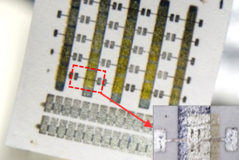
A KAIST team reported ultra-flexible organic flash memory that is bendable down to a radius of 300 ?μm. The memory exhibits a significantly-long projected retention rate with a programming voltage on par with the present industrial standards. A joint research team led by Professor Seunghyup Yoo of the School of Electrical Engineering and Professor Sung Gap Im of the Department of Chemical and Biomolecular Engineering said that their memory technology can be applied to non-conventional substrates, such as plastics and papers, to demonstrate its feasibility over a wide range of applications. With Dr. Seungwon Lee and Dr. Hanul Moon playing the role of leading authors, the research was published in Nature Communications on September 28. Flash memory is a non-volatile, transistor-based data-storage device that has become essential in most electronic systems in daily life. With straightforward operation mechanisms and easy integration into NAND or NOR array architecture, flash memory has been established as the most successful and dominant non-volatile memory technology by far. Despite promising demonstrations in the early stages of organic electronics, the overall progress in this field has been far slower than that of thin-film transistors (TFTs) or other devices based on flexible materials. It has been challenging, in particular, to develop flash memory that simultaneously exhibits a significant level of flexibility and performance. This is mainly due to the scarcity of flexible dielectric layers, which are responsible for the tunneling and blocking of charges. The solution processing used for the preparation of most of the polymeric dielectric layers also makes it difficult to use them in flash memory due to the complexity involved in the formation of the bilayer dielectric structure, which is the key to flash memory operations. The research team tried to overcome these hurdles and realize highly flexible flash memory by employing thin polymeric insulators grown with initiated chemical vapor deposition (iCVD), a vapor-phase growth technique for polymers that was previously shown to be promising for the fabrication of flexible TFTs. It was further shown that these iCVD-based polymeric insulators, when coupled with rational device design and material choice, can make a significant contribution to flash memory as well. Memory using conventional polymer insulating films has often required a voltage as high as 100 V (volt) in order to attain long memory retention. If the device is made to operate at a low voltage, the short retention period of less than a month was problematic. The KAIST team produced flash memory with programming voltages around 10 V and a projected data retention time of over 10 years, while maintaining its memory performance even at a mechanical strain of 2.8%. This is a significant improvement over the existing inorganic insulation layer-based flash memory that allowed only a 1% strain. The team demonstrated the virtually foldable memory devices by fabricating the proposed flash memory on a 6-micrometer-thick ultrathin plastic film. In addition, it succeeded in producing them on printing paper, opening a way for disposable smart electronic products such as electronic paper and electronic business card. Professor Yoo said, " This study well illustrates that even highly flexible flash memory can be made to have a practically viable level of performance, so that it contributes to full-fledged wearable electronic devices and smart electronic paper." < Figure 1. Structure of flexible flash memory > < Figure 2. Foldable flash memory >
-
Development of a Highly-Accurate Computational Mod..
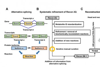
A research team from KAIST developed a computational framework that enables the reconstruction of a comprehensive computational model of human metabolism, which allows for an accurate prediction of personal metabolic features (or phenotypes). Understanding personal metabolic phenotypes allows us to design effective therapeutic strategies for various chronic and infectious diseases. A human computational model called the genome-scale metabolic model (GEM) contains information on thousands of metabolic genes and their corresponding reactions and metabolites, and has played an important role in predicting metabolic phenotypes. Although several versions of human GEMs have been released, they had room for further development, especially as to incorporating biological information coming from a human genetics mechanism called “alternative splicing.” Alternative splicing is a genetic mechanism that allows a gene to give rise to multiple reactions, and is strongly associated with pathology. To tackle this problem, Jae Yong Ryu (a Ph.D. student), Dr. Hyun Uk Kim (Research Fellow), and Distinguished Professor Sang Yup Lee, all from the Department of Chemical and Biomolecular Engineering at KAIST, developed a computational framework that systematically generates metabolic reactions, and adds them to the human GEM. The resulting human GEM was demonstrated to accurately predict metabolic phenotypes under varied environmental conditions. The research results were published online in Proceedings of the National Academy of Sciences (PNAS) on October 24, 2017, under the title “Framework and resource for more than 11,000 gene-transcript-protein-reaction associations in human metabolism.” The research team first updated the biological contents of a previous version of the human GEM. The updated biological contents include metabolic genes and their corresponding metabolites and reactions. In particular, metabolic reactions catalyzed by already-known protein isoforms were additionally incorporated into the human GEM; protein isoforms are multiple variants of proteins generated from individual genes through the alternative splicing process. Each protein isoform is often responsible for the operation of a metabolic reaction. Although multiple protein isoforms generated from one gene can play different functions by having different sets of protein domains and/or subcellular localizations, such information was not properly considered in previous versions of human GEMs. Upon the initial update of the human GEM, named Recon 2M.1, the research team subsequently implemented a computational framework that systematically generates information on Gene-Transcript-Protein-Reaction Associations (GeTPRA) in order to identify protein isoforms that were previously not identified. This framework was developed in this study. As a result of the implementation of the framework for GeTPRA, more than 11,000 GeTPRA were automatically predicted, and thoroughly validated. Additional metabolic reactions were then added to Recon 2M.1 based on the predicted GeTPRA for the previously uncharacterized protein isoforms; Recon 2M.1 was renamed Recon 2M.2 from this upgrade. Finally, Recon 2M.2 was integrated with 446 sets of personal biological data (RNA-Seq data) in order to build patient-specific cancer models. These patient-specific cancer models were used to predict cancer metabolism activities and anticancer targets. The development of a new version of human GEMs along with the computational framework for GeTPRA is expected to boost studies in fundamental human genetics and medicine. Model files of the human GEMs Recon 2M.1 and 2M.2, a full list of the GeTPRA and the source code for the computational framework to predict the GeTPRA are all available as part of the publication of this study. Distinguished Professor Lee said, “The predicted GeTPRA from the computational framework is expected to serve as a guideline for future experiments on human genetics and biochemistry, whereas the resulting Recon 2M.2 can be used to predict drug targets for various human diseases.” This work was supported by the Technology Development Program to Solve Climate Changes on Systems Metabolic Engineering for Biorefineries (NRF-2012M1A2A2026556 and NRF-2012M1A2A2026557) from the Ministry of Science and ICT through the National Research Foundation (NRF) of Korea. < Figure 1: A scheme of Recon 2M.1 development and its use in reconstructing personal genome-scale metabolic models (GEMs). (A) A concept of alternative splicing of human genes and its use in Gene-Transcript-Protein-Reaction Associations (GeTPRA) of Recon 2M.1. (B) A procedure of systematic refinement of the Recon 2Q. Recon 2Q is one of the previously released human GEMs. Biochemically inconsistent reactions include unbalanced, artificial, blocked, and/or redundant reactions. Iterative manual curation was conducted while validating the Recon 2M.1. (C) Reconstruction of cancer patient-specific GEMs using Recon 2M.1 for further simulation studies. In this study, personal biological data (RNA-Seq data) were obtained from The Cancer Genome Atlas (TCGA; https://cancergenome.nih.gov/ ) across the ten cancer types. > < Figure 2: Computational framework for the systematic generation of Gene-Transcript-Protein-Reaction Associations (GeTPRA; red box in the flowchart). Peptide sequences of metabolic genes defined in Recon 2M.1 were retrieved from a database called Ensembl. EC numbers and subcellular localizations of all the protein isoforms of metabolic genes in Recon 2M.1 were predicted using software programs EFICAz2.5 and Wolf PSort, respectively. Information on the newly predicted GeTPRA was systematically incorporated into the Recon 2M.1, thereby resulting in Recon 2M.2. >
-
Platinum Single Atom Catalysts for ‘Direct Formic ..
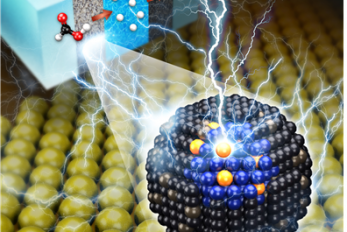
〈 Professor Hyunjoo Lee (left) and Ph.D. candidate Jiwhan Kim 〉 A research team co-led by Professor Hyunjoo Lee at the Department of Chemical and Biomolecular Engineering at KAIST and Professor Jeong Woo Han from the University of Seoul synthesized highly stable high-Pt-content single atom catalysts for direct formic acid fuel cells. The amount of platinum can be reduced to 1/10 of that of conventional platinum nanoparticle catalysts. Platinum (Pt) catalysts have been used in various catalytic reactions due to their high activity and stability. However, because Pt is rare and expensive, it is important to reduce the amount of Pt used. Pt single atom catalysts can reduce the size of the Pt particles to the size of an atom. Thus, the cost of Pt catalysts can be minimized because all of the Pt atoms can participate in the catalytic reactions. Additionally, single atom catalysts have no ensemble site in which two or more atoms are attached, and thus, the reaction selectivity is different from that of nanoparticle catalysts. Despite these advantages, single atom catalysts are easily aggregated and less stable due to their low coordination number and high surface free energy. It is difficult to develop a single atom catalyst with high content and high stability, and thus, its application in practical devices is limited. Direct formic acid fuel cells can be an energy source for next-generation portable devices because liquid formic acid as a fuel is safer and easier to store and transport than high-pressure hydrogen gas. To improve the stability of Pt single atom catalysts, Professor Lee’s group developed a Pt-Sn single atom alloy structure on an antimony-doped tin oxide (ATO) support. This structure has been proven by computational calculations which show that Pt single atoms substitute antimony sites in the antimony-tin alloy structure and are thermodynamically stable. This catalyst has been shown to have a higher activity up to 50 times per weight of Pt than that of the commercial catalyst, Pt/C, in the oxidation of formic acid, and the stability of the catalyst was also remarkably high. Professor Lee’s group also used a single atomic catalyst in a 'direct formic acid fuel cell’ consisting of membranes and electrodes. It is the first attempt to apply a single atomic catalyst to a full cell. In this case, an output similar to that of the commercial catalyst could be obtained by using 1/10 of the platinum compared to the commercial Pt/C catalyst. Ph.D. candidate Jiwhan Kim from KAIST was the first author of the research. This research was published online on September 11 in Advanced Energy Materials. This research was carried out with the support of the Samsung Electronics Future Technology Development Center. < Figure 1. Concept photograph for Pt single atom catalysts. > < Figure 2. Pt single atom catalysts by HAADF-STEM analysis (bright white circles) >
-
Professor Dai Gil Lee Recognized by the ICCS
Emeritus Professor Dai Gil Lee, from the School of Mechanical and Aerospace Engineering at KAIST, received a special achievement award from the 20th International Conference on Composite Structures (ICCS). ICCS is a renowned conference in the field of applied composite structures, which highlights the practicality of composite structures. This year, the conference was held at the Conservatoire National des Arts et M?tiers (CNAM), Paris, France from September 4 to 7. Approximately 650 papers were presented from 45 countries. Especially, the conference honored Emeritus Professor Lee, who has been engaged in ICCS since 1993 and received best paper award twice. The ICCS recognized him for serving with distinction in science and technology in the fields of composite materials and structures. As a member of the Editorial Board for many years, he gave significant support to the journal Composite Structures. At the conference, he gave a special lecture titled ‘Lightweight Carbon Composite Proton Exchange Membrane Fuel Cells’. Professor Lee said, “I will dedicate myself to innovate Vanadium Redox Flow Battery-ESS (VRFB) based on the research findings announced at the conference and related patents. I am hoping that these efforts will contribute to solving energy issues around the world.”
-
Highly Sensitive and Fast Indoor GNSS Signal Acqui..
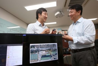
< Professor Seung-Hyun Kong (right) and Research Fellow Tae-Sun Kim> A research team led by Professor Seung-Hyun Kong at the Cho Chun Shik Graduate School of Green Transportation, KAIST, developed high-speed, high-sensitivity Global Navigation Satellite System (GNSS) signal acquisition (search and detection) technology that can produce GNSS positioning fixes indoors. Using the team’s new technology, GNSS signals will be sufficient to identify locations anywhere in the world, both indoors and outdoors. This new research finding was published in the international journal IEEE Signal Processing Magazine (IEEE SPM) this September. Global Positioning System (GPS) developed by the U.S. Department of Defense in the 1990s is the most widely-used satellite-based navigation system, and GNSS is a terminology to indicate conventional satellite based navigation systems, such as GPS and Russian GLONASS, as well as new satellite-based navigation systems under development, such as European GALILEO, Chinese COMPASS, and other regional satellite-based navigation systems. In general, GNSS signals are transmitted all over the globe from 20,000 km above the Earth and thus a GNSS signal received by a small antennae in an outdoor environment has weak signal power. In addition, GNSS signals penetrating building walls become extremely weak so the signal can be less than 1/1000th of the signal power received outside. Using conventional acquisition techniques including the frequency-domain correlation technique to acquire an extremely weak GNSS signal causes the computational cost to increase by over a million times and the processing time for acquisition also increases tremendously. Because of this, indoor measurement techniques using GNSS signals were considered practically impossible for the last 20 years. To resolve such limitations, the research team developed a Synthesized Doppler-frequency Hypothesis Testing (SDHT) technique to dramatically reduce the acquisition time and computational load for extremely weak GNSS signals indoors. In general, GNSS signal acquisition is a search process in which the instantaneous accurate code phase and Doppler frequency of the incoming GNSS signal are identified. However, the number of Doppler frequency hypotheses grows proportionally to the coherent correlation time that should be necessarily increased to detect weak signals. In practice, the coherent correlation time should be more than 1000 times longer for extremely weak GNSS signals so the number of Doppler frequency hypotheses is greater than 20,000. On the other hand, the SDHT algorithm indirectly tests the Doppler frequency hypothesis utilizing the coherent correlation results of neighboring hypotheses. Therefore, using SDHT, only around 20 hypotheses are tested using conventional correlation techniques and the remaining 19,980 hypotheses are calculated with simple mathematical operations. As a result, SDHT achieves a huge computational cost reduction (by about 1000 times) and is 800 times faster for signal acquisition compared to conventional techniques. This means only about 15 seconds is required to detect extremely weak GNSS signals in buildings using a personal computer. The team predicts further studies for strengthening SDHT technology and developing positioning systems robust enough to multipath in indoor environments will allow indoor GNSS measurements within several seconds inside most buildings using GNSS alone. Professor Kong said, “This development made us the leader in indoor GNSS positioning technology in the world.” He continued, “We hope to commercialize indoor GNSS systems to create a new market.” The research team is currently registering a patent in Korea and applying for patents overseas, as well as planning to commercialize the technology with the help of the Institute for Startup KAIST. < Figure1. Positioning Results for the GPS Indoor Positioning System using SDHT Technology >
-
Ultra-Fast and Ultra-Sensitive Hydrogen Sensor
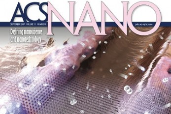
A KAIST team made an ultra-fast hydrogen sensor that can detect hydrogen gas levels under 1% in less than seven seconds. The sensor also can detect hundreds of parts per million levels of hydrogen gas within 60 seconds at room temperature. A research group under Professor Il-Doo Kim in the Department of Materials Science and Engineering at KAIST, in collaboration with Professor Reginald M. Penner of the University of California-Irvine, has developed an ultra-fast hydrogen gas detection system based on a palladium (Pd) nanowire array coated with a metal-organic framework (MOF). Hydrogen has been regarded as an eco-friendly next-generation energy source. However, it is a flammable gas that can explode even with a small spark. For safety, the lower explosion limit for hydrogen gas is 4 vol% so sensors should be able to detect the colorless and odorless hydrogen molecule quickly. The importance of sensors capable of rapidly detecting colorless and odorless hydrogen gas has been emphasized in recent guidelines issued by the U.S. Department of Energy. According to the guidelines, hydrogen sensors should detect 1 vol% of hydrogen in air in less than 60 seconds for adequate response and recovery times. To overcome the limitations of Pd-based hydrogen sensors, the research team introduced a MOF layer on top of a Pd nanowire array. Lithographically patterned Pd nanowires were simply overcoated with a Zn-based zeolite imidazole framework (ZIF-8) layer composed of Zn ions and organic ligands. ZIF-8 film is easily coated on Pd nanowires by simple dipping (for 2?6 hours) in a methanol solution including Zn (NO3)2·6H2O and 2-methylimidazole. < This cover image depicts lithographically-patterned Pd nanowires overcoated with a Zn-based zeolite imidazole framework (ZIF-8) layer. > As synthesized ZIF-8 is a highly porous material composed of a number of micro-pores of 0.34 nm and 1.16 nm, hydrogen gas with a kinetic diameter of 0.289 nm can easily penetrate inside the ZIF-8 membrane, while large molecules (> 0.34 nm) are effectively screened by the MOF filter. Thus, the ZIF-8 filter on the Pd nanowires allows the predominant penetration of hydrogen molecules, leading to the acceleration of Pd-based H2 sensors with a 20-fold faster recovery and response speed compared to pristine Pd nanowires at room temperature. Professor Kim expects that the ultra-fast hydrogen sensor can be useful for the prevention of explosion accidents caused by the leakage of hydrogen gas. In addition, he expects that other harmful gases in the air can be accurately detected through effective nano-filtration by using of a variety of MOF layers. This study was carried out by Ph.D. candidate Won-Tae Koo (first author), Professor Kim (co-corresponding author), and Professor Penner (co-corresponding author). The study has been published in the online edition of ACS Nano, as the cover-featured image for the September issue. < Figure 1. Representative image for this paper published in ACS Nano, August, 18. > < Figure 2. Images of Pd nanowire array-based hydrogen sensors, scanning electron microscopy image of a Pd nanowire covered by a metal-organic framework layer, and the hydrogen sensing properties of the sensors. > < Figure 3. Schematic illustration of a metal-organic framework (MOF). The MOF, consisting of metal ions and organic ligands, is a highly porous material with an ultrahigh surface area. The various structures of MOFs can be synthesized depending on the kinds of metal ions and organic ligands. > < (From left) Professor Kim, Ph.D. candidate Koo, and Professor Penner >
-
Sangeun Oh Recognized as a 2017 Google Fellow
Sangeun Oh, a Ph.D. candidate in the School of Computing was selected as a Google PhD Fellow in 2017. He is one of 47 awardees of the Google PhD Fellowship in the world. The Google PhD Fellowship awards students showing outstanding performance in the field of computer science and related research. Since being established in 2009, the program has provided various benefits, including scholarships worth $10,000 USD and one-to-one research discussion with mentors from Google. His research work on a mobile system that allows interactions among various kinds of smart devices was recognized in the field of mobile computing. He developed a mobile platform that allows smart devices to share diverse functions, including logins, payments, and sensors. This technology provides numerous user experiences that existing mobile platforms could not offer. Through cross-device functionality sharing, users can utilize multiple smart devices in a more convenient manner. The research was presented at The Annual International Conference on Mobile Systems, Applications, and Services (MobiSys) of the Association for Computing Machinery in July, 2017. Oh said, “I would like to express my gratitude to my advisor, the professors in the School of Computing, and my lab colleagues. I will devote myself to carrying out more research in order to contribute to society.” His advisor, Insik Shin, a professor in the School of Computing said, “Being recognized as a Google PhD Fellow is an honor to both the student as well as KAIST. I strongly anticipate and believe that Oh will make the next step by carrying out good quality research.”
-

Humicotta Wins the Silver Prize at the 2017 IDEA
The 3D-printed ceramic humidifier made by the research team led by Professor Sang-Min Bae won the silver prize at the 2017 International Design Excellence Awards (IDEA). Professor Bae’s ID+IM team was also listed as winners of three more appropriate technology designs at the IDEA. The awards, sponsored by the Industrial Designers Society of America, are one of the three prestigious design awards including the Red Dot Design Award and the iF Design Award in Germany. The silver prize winner in the category of home and bath, Humicotta is an energy-efficient, bacteria free, and easy to clean humidifier. It includes a base module and filter. The base is a cylindrical pedestal with a built-in fan on which the filter is placed. The filter is a 3D-printed honeycomb structure made of diatomite. When water is added, the honeycomb structure and porous terracotta maximize natural humidification. It also offers an open platform service that customizes the filters or provides files that users can use their own 3D printer. Professor Bae’s team has worked on philanthropy design using appropriate technology as their main topic for years. Their designs have been recognized at prestigious global design awards events, winning more than 50 prizes with innovative designs made for addressing various global and social problems including the following innovations. The Light Funnel is a novel type of lighting device designed for off-grid areas of Africa. It helps to maximize the natural light effect in the daytime without any drastic home renovations. It consists of a transparent acrylic sphere and a reflective pathway. After filling the acrylic sphere with water and placing it on a rooftop, sunlight passes into the house through the water inside the sphere. It provides a lighted environment nine times brighter than without it. Also, once installed, it can be used almost permanently. The Maasai Smart Cane is made using wood sticks purchased through fair trade with the Maasai tribe. GPS is installed into the grip of the birch-tree cane, so that cane users can send a signal when in an emergency situation. All of the proceeds of this product go to the tribe. S.Cone is a first aid kit made in collaboration with Samsung Fire and Marine Insurance. The traffic cone-shaped kit is designed to help users handle an emergency situation intact and safe. The S.Cone has unique versions for fires, car accidents, and marine accidents. For example, the S.Cone for fires is equipped with a small fire extinguisher, smoke mask, and fire blanket. The cap of the S.Cone also functions as an IoT station connecting the fire and gas detector with smart phones. Professor Bae said of his team’s winning design products, “By making the data public, any person can design their own humidifier if they have access to a 3D-printer. We want it to be a very accessible product for the public. The Light Funnel and Maasai Smart Cane are designed for economically-marginalized populations and the elderly. We will continue to make the best designed products serving the marginalized 90% of the population around the world.”
-

Professor Jun Ho Oh’s Total Solar Eclipse Featured..
< Professor Jun Ho Oh > A video of a total solar eclipse, filmed in Warm Springs, Oregon by Professor Jun Ho Oh of the Department of Mechanical Engineering, was selected as the Astronomy Picture of the Day (APOD). APOD, is a NASA website specializing in astronomy pictures. It features astronomical observations recorded by the Hubble Space Telescope or photos taken by astronomical observers from around the world. Professor Oh is now the second Korean and the first amateur photographer whose photo was selected as the APOD. According to the website, ‘the video frames were acquired with equipment specifically designed by Jun Ho Oh to track a close-up of the Sun’s periphery during the eclipse.’ Also, Digital Photography Review (dpreview.com) introduced observation points of the eclipse in his three-minute video, including solar prominences, corona, and Baily’s beads. Professor Oh, the creator of the bipedal walking humanoid robot named Hubo, has been chasing eclipse since his first trip to Turkey in 1999. “After numerous trials and failures over the last 18 years, I was finally able to capture every single breath-taking moment of the total eclipse,” said the professor. He’s already planning for the next total eclipse in Chile on July 2, 2019. Click the link to watch the video https://apod.nasa.gov/apod/ap170912.html < #1 Photo of solar eclipse > < #2 Photo of solar eclipse >
-
Semiconductor Patterning of Seven Nanometers Techn..
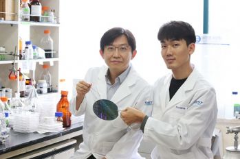
A research team led by Professor Sang Ouk Kim in the Department of Materials Science and Engineering at KAIST has developed semiconductor manufacturing technology using a camera flash. This technology can manufacture ultra-fine patterns over a large area by irradiating a single flash with a seven-nanometer patterning technique for semiconductors. It can facilitate the manufacturing of highly efficient, integrated semiconductor devices in the future. Technology for the Artificial Intelligence (AI), the Internet of Things (IoTs), and big data, which are the major keys for the fourth Industrial Revolution, require high-capacity, high-performance semiconductor devices. It is necessary to develop lithography technology to produce such next-generation, highly integrated semiconductor devices. Although related industries have been using conventional photolithography for small patterns, this technique has limitations for forming a pattern of sub-10 nm patterns.? Molecular assembly patterning technology using polymers has been in the spotlight as the next generation technology to replace photolithography because it is inexpensive to produce and can easily form sub-10 nm patterns. However, since it generally takes a long time for heat treatment at high-temperature or toxic solvent vapor treatment, mass production is difficult and thus its commercialization has been limited. The research team introduced a camera flash that instantly emits strong light to solve the issues of polymer molecular assembly patterning. Using a flash can possibly achieve a semiconductor patterning of seven nanometers within 15 milliseconds (1 millisecond = 1/1,000 second), which can generate a temperature of several hundred degrees Celsius in several tens of milliseconds. The team has demonstrated that applying this technology to polymer molecular assembly allows a single flash of light to form molecular assembly patterns. The team also identified its compatibility with polymer flexible substrates, which are impossible to process at high temperatures. Through these findings, the technology can be applied to the fabrication of next-generation, flexible semiconductors. The researchers said the camera flash photo-thermal process will be introduced into molecular assembly technology and this highly-efficiency technology can accelerate the realization of molecular assembly semiconductor technology. Professor Kim, who led the research, said, “Despite its potential, molecular assembly semiconductor technology has remained a big challenge in improving process efficiency.” “This technology will be a breakthrough for the practical use of molecular assembly-based semiconductors.” The paper was published in the international journal, Advanced Materials on August 21 with first authors, researcher Hyeong Min Jin and PhD candidate Dae Yong Park. The research, sponsored by the Ministry of Science and ICT, was co-led Professor by Keon Jae Lee in the Department of Materials Science and Engineering at KAIST, and Professor Kwang Ho Kim in the School of Materials Science and Engineering at Pusan National University. < 1. Formation of semiconductor patterns using a camera flash> < Schematic diagram of molecular assembly pattern using a camera flash > < Self-assembled patterns>
-
A Novel and Practical Fab-route for Superomniphobi..
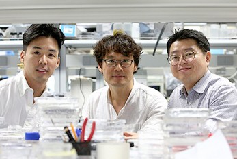
(clockwise from left: Jaeho Choi, Hee Tak Kim, Shin-Hyun Kim) A joint research team led by Professor Hee Tak Kim and Shin-Hyun Kim in the Department of Chemical and Biomolecular Engineering at KAIST developed a fabrication technology that can inexpensively produce surfaces capable of repelling liquids, including water and oil. The team used the photofluidization of azobenzene molecule-containing polymers to generate a superomniphobic surface which can be applied for developing stain-free fabrics, non-biofouling medical tubing, and corrosion-free surfaces. Mushroom-shaped surface textures, also called doubly re-entrant structures, are known to be the most effective surface structure that enhances resistance against liquid invasion, thereby exhibiting superior superomniphobic property. However, the existing procedures for their fabrication are highly delicate, time-consuming, and costly. Moreover, the materials required for the fabrication are restricted to an inflexible and expensive silicon wafer, which limits the practical use of the surface. To overcome such limitations, the research team used a different approach to fabricate the re-entrant structures called localized photofludization by using the peculiar optical phenomenon of azobenzene molecule-containing polymers (referred to as azopolymers). It is a phenomenon where an azopolymer becomes fluidized under irradiation, and the fluidization takes place locally within the thin surface layer of the azopolymer. With this novel approach, the team facilitated the localized photofluidization in the top surface layer of azopolymer cylindrical posts, successfully reconfiguring the cylindrical posts to doubly re-entrant geometry while the fluidized thin top surface of an azopolymer is flowing down. The structure developed by the team exhibits a superior superomniphobic property even for liquids infiltrating the surface immediately. Moreover, the superomniphobic property can be maintained on a curved target surface because its surficial materials are based on high molecules. Furthermore, the fabrication procedure of the structure is highly reproducible and scalable, providing a practical route to creating robust omniphobic surfaces. Professor Hee Tak Kim said, “Not only does the novel photo-fluidization technology in this study produce superior superomniphobic surfaces, but it also possesses many practical advantages in terms of fab-procedures and material flexibility; therefore, it could greatly contribute to real uses in diverse applications.” Professor Shin-Hyun Kim added, “The designed doubly re-entrant geometry in this study was inspired by the skin structure of springtails, insects dwelling in soil that breathe through their skin. As I carried out this research, I once again realized that humans can learn from nature to create new engineering designs.” The paper (Jaeho Choi as a first author) was published in ACS Nano, an international journal for Nano-technology, in August. < Schematic diagram of mushroom-shaped structure fabrication > < SEM image of mushroom-shaped structure > < Image of superomniphobic property of different types of liquid >

