


News
College of Engineering News
-

Prof. Jung-Ryul Lee Honored with 2024 KSCM Academ..
Prof. Jung-RyulLee received 2024 Academic Achievement Award from the Korean Society for Composite Materials (KSCM) during its annual fall conference. This award is the most prestigious honor that the society can bestow, recognizing a lifetime of distinguished achievement in the field of composite materials. The award ceremony took place on November 14 at the Busan Port Int’l Exhibition & Convention Center (BPEX). This award acknowledges Prof. Lee’s dedicated research efforts in non-destructive testing of composite materials, design of radar-absorbing structures, and defect detection and monitoring in composite structures.
-
KAIST’s Beach-Roaming Quadrupedal Robot “RAIBO” to..
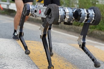
“RAIBO”, KAIST’s four-legged robot featuring remarkable agility even on challenging terrains like sandy beaches, is now set to be the first in the world to complete a full marathon. < Photo 1. A group photo of the research team of Professor Je Min Hwangbo (second from the right in the front row) of the Department of Mechanical Engineering who participated in the marathon event at 2024 Geumsan Insam Festival last September > On the 17th of November, KAIST (represented by President Kwang Hyung Lee) announced that Professor Je Min Hwangbo’s team from the Department of Mechanical Engineering has developed an upgraded version, “RAIBO2,” which will take on the full 42.195-kilometer course at the "Sangju Dried-Persimmon Marathon". This is over double the previous maximum distance achieved by quadruped robots, which was limited to around 20 kilometers. The KAIST team has successfully developed a robot that can walk continuously for 43 kilometers on a single charge, completing the course in 4 hours and 40 minutes by following a GPS-guided path on the university’s main athletic field. Through this marathon, the team aims to demonstrate RAIBO2’s walking performance in an actual urban environment. Previously, most measurements of walking robots’ travel distances were confined to controlled laboratory conditions or theoretical data. This marathon challenge is thus significant in that the robot will run alongside the general public in a real urban setting, marking the first attempt to validate the practical potential of four-legged robots in real environments. Quadruped robots have shown advantages in challenging terrains, such as ice, sand, and mountainous areas, where they can walk stably. However, limited travel distance and running time have long been obstacles to wider applications. < Figure 1. Conceptual diagram of power flow employed by the quadruped robot > Professor Hwangbo’s team designed every component of the robot, from its actuators to its mechanical structure, to overcome these limitations. Notably, they implemented an efficient walking control system based on reinforcement learning using their proprietary dynamic simulator “RaiSim”. The team also collected and analyzed walking data from outdoor environments, creating a model to address walking losses. This model was then used to iteratively improve walking efficiency over one full year. < Figure 2. The leg posture change process of RAIBO2 walking at the most efficient walking speed of 3 m/s. By reducing the ground contact speed of the feet, the collision energy loss was reduced, and by minimizing the slipperiness of the foot upon contact, the body's kinetic energy was maintained towards the direction of the movement. > This is the team’s second attempt. Their first was during the marathon event at “Geumsan Insam Festival” in September when the robot’s battery ran out at the 37-kilometer mark, falling short of completion. The battery drained 10 kilometers earlier than expected due to frequent speed changes as the robot adjusted to the pacing of other runners on the course. Following the initial attempt, the team focused on technical improvements for a successful finish. They enhanced control efficiency by implementing joint stiffness control directly onto the motor actuator and increased battery capacity by 33% by refining the internal structure. These improvements enabled the robot to cover a maximum distance of 67 kilometers on straight paths. < Figure 3. Data from completing 43 km on a single charge at the main sports field on campus. Left) GPS data of the driving course used during autonomous running. Middle) Covered distance by the hour. Right) Energy consumption by module > Choongin Lee, a Ph.D. student of RAI Lab who is one of the co-first author of this study, explained, “Our comprehensive analysis of walking losses in terms of mechanics, electrical systems, and walking methods was crucial to improving walking efficiency. This research marks an important milestone in extending the operating range of quadruped robots to urban environments.” < Photo 2. A Photo from Practice Run> This research was supported by the Samsung Electronics Future Technology Development Center and RAION ROBOTICS Co., Ltd. < Photo 3. A Photo from Practice Run >
-
KAIST Researchers Suggest an Extraordinary Alterna..
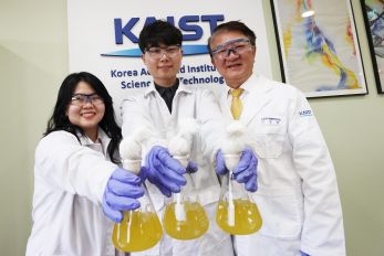
< (From left) Dr. Cindy Pricilia, Ph.D. Candidate Cheon Woo Moon, Distinguished Professor Sang Yup Lee > Currently, the world is suffering from environmental problems caused by plastic waste. The KAIST research team has succeeded in producing a microbial-based plastic that is biodegradable and can replace existing PET bottles, making it a hot topic. Our university announced on the 7th of November that the research team of Distinguished Professor Sang Yup Lee of the Department of Chemical and Biomolecular Engineering has succeeded in developing a microbial strain that efficiently produces pseudoaromatic polyester monomer to replace polyethylene terephthalate (PET) using systems metabolic engineering. Pseudoaromatic dicarboxylic acids have better physical properties and higher biodegradability than aromatic polyester (PET) when synthesized as polymers, and are attracting attention as an eco-friendly monomer* that can be synthesized into polymers. The production of pseudoaromatic dicarboxylic acids through chemical methods has the problems of low yield and selectivity, complex reaction conditions, and the generation of hazardous waste. *Monomer: A material for making polymers, which is used to synthesize polymers by polymerizing monomers together < Figure. Overview of pseudoaromatic dicarboxylic acid production using metabolically engineered C. glutamicum. > To solve this problem, Professor Sang Yup Lee's research team used metabolic engineering to develop a microbial strain that efficiently produces five types of pseudoaromatic dicarboxylic acids, including 2-pyrone-4,6-dicarboxylic acid and four types of pyridine dicarboxylic acids (2,3-, 2,4-, 2,5-, 2,6-pyridine dicarboxylic acids), in Corynebacterium, a bacterium mainly used for amino acid production. The research team used metabolic engineering techniques to build a platform microbial strain that enhances the metabolic flow of protocatechuic acid, which is used as a precursor for several pseudoaromatic dicarboxylic acids, and prevents the loss of precursors. Based on this, the genetic manipulation target was discovered through transcriptome analysis, producing 76.17 g/L of 2-pyrone-4,6-dicarboxylic acid, and by newly discovering and constructing three types of pyridine dicarboxylic acid production metabolic pathways, successfully producing 2.79 g/L of 2,3-pyridine dicarboxylic acid, 0.49 g/L of 2,4-pyridine dicarboxylic acid, and 1.42 g/L of 2,5-pyridine dicarboxylic acid. In addition, the research team confirmed the production of 15.01 g/L through the construction and reinforcement of the 2,6-pyridine dicarboxylic acid biosynthesis pathway, successfully producing a total of five similar aromatic dicarboxylic acids with high efficiency. In conclusion, the team succeeded in producing 2,4-, 2,5-, and 2,6-pyridine dicarboxylic acids at the world's highest concentration. In particular, 2,4-, 2,5-pyridine dicarboxylic acid achieved production on the scale of g/L, which was previously produced in extremely small amounts (mg/L). Based on this study, it is expected that it will be applied to various polyester production industrial processes, and it is also expected that it will be actively utilized in research on the production of similar aromatic polyesters. Professor Sang Yup Lee, the corresponding author, said, “The significance lies in the fact that we have developed an eco-friendly technology that efficiently produces similar aromatic polyester monomers based on microorganisms,” and “This study will help the microorganism-based bio-monomer industry replace the petrochemical-based chemical industry in the future.” The results of this study were published in the international academic journal, the Proceedings of the National Academy of Sciences of United States of America (PNAS) on October 30th. ※ Paper title: Metabolic engineering of Corynebacterium glutamicum for the production of pyrone and pyridine dicarboxylic acids ※ Author information: Jae Sung Cho (co-first author), Zi Wei Luo (co-first author), Cheon Woo Moon (co-first author), Cindy Prabowo (co-author), Sang Yup Lee (corresponding author) - a total of 5 people This study was conducted with the support of the Development of Next-generation Biorefinery Platform Technologies for Leading Bio-based Chemicals Industry Project and the Development of Platform Technologies of Microbial Cell Factories for the Next-generation Biorefineries Project (Project leader: Professor Sang Yup Lee) from the National Research Foundation supported by the Ministry of Science and Technology and ICT of Korea.
-
KAIST Researchers Introduce New and Improved, Next..
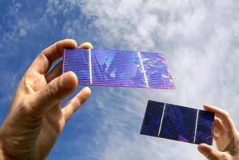
- KAIST-Yonsei university researchers developed innovative dipole technology to maximize near-infrared photon harvesting efficiency - Overcoming the shortcoming of existing perovskite solar cells that cannot utilize approximately 52% of total solar energy - Development of next-generation solar cell technology with high efficiency and high stability that can absorb near-infrared light beyond the existing visible light range with a perovskite-dipole-organic semiconductor hybrid structure < Photo. (From left) Professor Jung-Yong Lee, Ph.D. candidate Min-Ho Lee, and Master’s candidate Min Seok Kim of the School of Electrical Engineering > Existing perovskite solar cells, which have the problem of not being able to utilize approximately 52% of total solar energy, have been developed by a Korean research team as an innovative technology that maximizes near-infrared light capture performance while greatly improving power conversion efficiency. This greatly increases the possibility of commercializing next-generation solar cells and is expected to contribute to important technological advancements in the global solar cell market. The research team of Professor Jung-Yong Lee of the School of Electrical Engineering at KAIST (President Kwang-Hyung Lee) and Professor Woojae Kim of the Department of Chemistry at Yonsei University announced on October 31st that they have developed a high-efficiency and high-stability organic-inorganic hybrid solar cell production technology that maximizes near-infrared light capture beyond the existing visible light range. The research team suggested and advanced a hybrid next-generation device structure with organic photo-semiconductors that complements perovskite materials limited to visible light absorption and expands the absorption range to near-infrared. In addition, they revealed the electronic structure problem that mainly occurs in the structure and announced a high-performance solar cell device that dramatically solved this problem by introducing a dipole layer*. *Dipole layer: A thin material layer that controls the energy level within the device to facilitate charge transport and forms an interface potential difference to improve device performance. Existing lead-based perovskite solar cells have a problem in that their absorption spectrum is limited to the visible light region with a wavelength of 850 nanometers (nm) or less, which prevents them from utilizing approximately 52% of the total solar energy. To solve this problem, the research team designed a hybrid device that combined an organic bulk heterojunction (BHJ) with perovskite and implemented a solar cell that can absorb up to the near-infrared region. In particular, by introducing a sub-nanometer dipole interface layer, they succeeded in alleviating the energy barrier between the perovskite and the organic bulk heterojunction (BHJ), suppressing charge accumulation, maximizing the contribution to the near-infrared, and improving the current density (JSC) to 4.9 mA/cm². The key achievement of this study is that the power conversion efficiency (PCE) of the hybrid device has been significantly increased from 20.4% to 24.0%. In particular, this study achieved a high internal quantum efficiency (IQE) compared to previous studies, reaching 78% in the near-infrared region. < Figure. The illustration of the mechanism of improving the electronic structure and charge transfer capability through Perovskite/organic hybrid device structure and dipole interfacial layers (DILs). The proposed dipole interfacial layer forms a strong interfacial dipole, effectively reducing the energy barrier between the perovskite and organic bulk heterojunction (BHJ), and suppressing hole accumulation. This technology improves near-infrared photon harvesting and charge transfer, and as a result, the power conversion efficiency of the solar cell increases to 24.0%. In addition, it achieves excellent stability by maintaining performance for 1,200 hours even in an extremely humid environment. > In addition, this device showed high stability, showing excellent results of maintaining more than 80% of the initial efficiency in the maximum output tracking for more than 800 hours even under extreme humidity conditions. Professor Jung-Yong Lee said, “Through this study, we have effectively solved the charge accumulation and energy band mismatch problems faced by existing perovskite/organic hybrid solar cells, and we will be able to significantly improve the power conversion efficiency while maximizing the near-infrared light capture performance, which will be a new breakthrough that can solve the mechanical-chemical stability problems of existing perovskites and overcome the optical limitations.” This study, in which KAIST School of Electrical Engineering Ph.D. candidate Min-Ho Lee and Master's candidate Min Seok Kim participated as co-first authors, was published in the September 30th online edition of the international academic journal Advanced Materials. (Paper title: Suppressing Hole Accumulation Through Sub-Nanometer Dipole Interfaces in Hybrid Perovskite/Organic Solar Cells for Boosting Near-Infrared Photon Harvesting). This study was conducted with the support of the National Research Foundation of Korea.
-

Prof. Jae-Hung Han Honored with 2024 KSNVE Academ..
Prof. Jae-Hung Han received 2024 Academic Achievement Award from the Korean Society for Noise and Vibration Engineering (KSNVE) during its annual fall conference. The award is the most prestigious award that the society can bestow and is to recognize lifetime distinguished achievement in the sound and vibration area. The award ceremony took place on October 24 at the High1 Grand Hotel Convention Tower in Jeongseon, Gangwon Province. This award recognizes Prof. Han’s dedicated research efforts in aeroelastic vibration analysis, satellite micro-vibration isolation, and coupled load analysis for launch vehicles.
-
KAIST Professor Uichin Lee Receives Distinguished ..
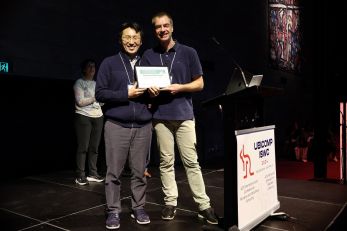
< Photo. Professor Uichin Lee (left) receiving the award > KAIST (President Kwang Hyung Lee) announced on the 25th of October that Professor Uichin Lee’s research team from the School of Computing received the Distinguished Paper Award at the International Joint Conference on Pervasive and Ubiquitous Computing and International Symposium on Wearable Computing (Ubicomp / ISWC) hosted by the Association for Computing Machinery (ACM) in Melbourne, Australia on October 8. The ACM Ubiquitous Computing Conference is the most prestigious international conference where leading universities and global companies from around the world present the latest research results on ubiquitous computing and wearable technologies in the field of human-computer interaction (HCI). The conference program is composed of invited papers published in the Proceedings of the ACM (PACM) on Interactive, Mobile, Wearable and Ubiquitous Technologies (IMWUT), which covers the latest research in the field of ubiquitous and wearable computing. The Distinguished Paper Award Selection Committee selected eight papers among 205 papers published in the seven volumes of the ACM Proceedings (PACM IMWUT) that made outstanding and exemplary contributions to the research community. The committee consists of 16 prominent experts who are current and former members of the journal's editorial board which made the selection after a rigorous review of all papers for a period that stretched over a month. < Figure 1. BeActive mobile app to promote physical activity to form active lifestyle habits > The research that won the Distinguished Paper Award was conducted by Dr. Junyoung Park, a graduate of the KAIST Graduate School of Data Science, as the 1st author, and was titled “Understanding Disengagement in Just-in-Time Mobile Health Interventions” Professor Uichin Lee’s research team proposed ‘Just-in-Time (JIT) Mobile Health Interventions’ that actively provide interventions in optimal situations by utilizing data collected from health management apps, based on the premise that these apps are aptly in use to ensure effectiveness. < Figure 2. Overview of traditional user-requested digital behavioral intervention notifications (Pull) and automatic transmission (Push) for Just-in-Time (JIT) mobile health interventions using smartphone sensing technologies > The research team conducted a systematic analysis of the decline in participation in digital behavior change interventions. They developed the BeActive system, an app that promotes physical activities designed to help forming active lifestyle habits, and systematically analyzed the effects of users’ self-control ability and boredom-proneness on compliance with behavioral interventions. The results of an 8-week empirical experiment revealed that even if JIT interventions are provided according to the user’s situation, it is impossible to avoid a decline in participation. However, for users with high self-control and low boredom tendency, the compliance with JIT interventions delivered through the app was significantly higher than that of users in other groups. In particular, users with high boredom proneness easily got tired of the repeated timely interventions, and their compliance with the app decreased more quickly than in other groups. < Figure 3. JIT Mobile Health Intervention: a demonstrative case of the BeActive system > Professor Uichin Lee explained, “The results of the first study on the participation in digital therapeutics and wellness services utilizing JIT mobile health interventions provide a starting point for exploring ways to increase participation,” and “It will be possible to develop user-centered artificial intelligence technology that increases participation by utilizing large-scale language models (LLMs) and complex situational awareness technologies.” < Figure 4. A conceptual illustration of engagement in digital health apps. Engagement in digital health apps consists of (1) engagement in using digital health apps and (2) engagement in behavioral interventions provided by digital health apps, i.e., compliance with behavioral interventions. Adherence to behavioral interventions recommended by digital health apps can help achieve the ultimate health goals. > This study was conducted with the support of the 2021 Biomedical Technology Development Program and the 2022 Basic Research and Development Program of the National Research Foundation of Korea funded by the Ministry of Science and ICT. < Figure 5. A conceptual illustration of participation and disengagement. It is divided into participation by use of service provided by the app and participation (adherence) for behavioral intervention. The distinction of participation can be explained by dividing it into adoption, abandonment, and attrition. > < Figure 6. Trends of changes in frequency of app usage and adherence to behavioral intervention over 8 weeks, ● SC: Self-Control Ability (High-SC: user group with high self-control, Low-SC: user group with low self-control) ● BD: Boredom-Proneness (High-BD: user group with high boredom-proneness, Low-BD: user group with low boredom-proneness) >
-
KAIST Develops Thread-like, Flexible Thermoelectri..
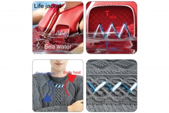
A thermoelectric material that can be used in wearable devices such as smart clothing and maintains stable thermal energy performance even in extreme environments has been developed by a team of Korean researchers. It has dramatically resolved the dilemma of striking the balance between achieving good performance and the mechanical flexibility of thermoelectric materials, which has been a long-standing challenge in the field of thermoelectric materials, and has also proven the possibility of commercialization. KAIST (President Kwang-Hyung Lee) announced on the 21st that a joint research team of Professor Yeon Sik Jung of the Department of Materials Science and Engineering and Professor Inkyu Park of the Department of Mechanical Engineering, in collaboration with the research teams of Professor Min-Wook Oh of Hanbat National University (President Yong Jun Oh) and Dr. Jun-Ho Jeong of the Korea Institute of Machinery and Materials (President Seoghyun Ryu), have successfully developed ‘bismuth telluride (Bi2Te3) thermoelectric fibers,’ an innovative energy harvesting solution for next-generation flexible electronic devices. Thermoelectric materials are materials that generate voltage when there is a temperature difference and convert thermal energy into electrical energy. Currently, about 70% of energy being lost as wasted heat, so due attention is being given to research on these as sustainable energy materials that can recover and harvesting energy from this waste heat. Most of the heat sources around us are curved, such as the human body, vehicle exhaust pipes, and cooling fins. Inorganic thermoelectric materials based on ceramic materials boast high thermoelectric performance, but they are fragile and difficult to produce in curved shapes. On the other hand, flexible thermoelectric materials using existing polymer binders can be applied to surfaces of various shapes, but their performance was limited due to the low electrical conductivity and high thermal resistance of the polymer. Existing flexible thermoelectric materials contain polymer additives, but the inorganic thermoelectric material developed by the research team is not flexible, so they overcame these limitations by twisting nano ribbons instead of additives to produce a thread-shaped thermoelectric material. Inspired by the flexibility of inorganic nano ribbons, the research team used a nanomold-based electron beam deposition technique to continuously deposit nano ribbons and then twisted them into a thread shape to create bismuth telluride (Bi2Te3) inorganic thermoelectric fibers. These inorganic thermoelectric fibers have higher bending strength than existing thermoelectric materials, and showed almost no change in electrical properties even after repeated bending and tensile tests of more than 1,000 times. The thermoelectric device created by the research team generates electricity using temperature differences, and if clothes are made with fiber-type thermoelectric devices, electricity can be generated from body temperature to operate other electronic devices. < Figure 1. Schematic diagram and actual image of the all-inorganic flexible thermoelectric yarn made without polymer additives > In fact, the possibility of commercialization was proven through a demonstration of collecting energy by embedding thermoelectric fibers in life jackets or clothing. In addition, it opened up the possibility of building a high-efficiency energy harvesting system that recycles waste heat by utilizing the temperature difference between the hot fluid inside a pipe and the cold air outside in industrial settings. Professor Yeon Sik Jung said, "The inorganic flexible thermoelectric material developed in this study can be used in wearable devices such as smart clothing, and it can maintain stable performance even in extreme environments, so it has a high possibility of being commercialized through additional research in the future." Professor Inkyu Park also emphasized, "This technology will become the core of next-generation energy harvesting technology, and it is expected to play an important role in various fields from waste heat utilization in industrial sites to personal wearable self-power generation devices." This study, in which Hanhwi Jang, a Ph.D. student at KAIST's Department of Materials Science and Engineering, Professor Junseong Ahn of Korea University, Sejong Campus, and Dr. Yongrok Jeong of Korea Atomic Energy Research Institute contributed equally as joint first authors, was published in the online edition of the international academic journal Advanced Materials on September 17, and was selected as the back-cover paper in recognition of its excellence. (Paper title: Flexible All-Inorganic Thermoelectric Yarns) Meanwhile, this study was conducted through the Mid-career Researcher Support Program and the Future Materials Discovery Program of the National Research Foundation of Korea, and the support from the Global Bio-Integrated Materials Center, the Ministry of Trade, Industry and Energy, and the Korea Institute of Industrial Technology Evaluation and Planning (KEIT) upon the support by the Ministry of Science and ICT.
-
KAIST Develops Technology for the Precise Diagnosi..
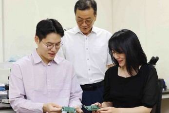
Accurately diagnosing the state of electric vehicle (EV) batteries is essential for their efficient management and safe use. KAIST researchers have developed a new technology that can diagnose and monitor the state of batteries with high precision using only small amounts of current, which is expected to maximize the batteries’ long-term stability and efficiency. KAIST (represented by President Kwang Hyung Lee) announced on the 17th of October that a research team led by Professors Kyeongha Kwon and Sang-Gug Lee from the School of Electrical Engineering had developed electrochemical impedance spectroscopy (EIS) technology that can be used to improve the stability and performance of high-capacity batteries in electric vehicles. EIS is a powerful tool that measures the impedance* magnitude and changes in a battery, allowing the evaluation of battery efficiency and loss. It is considered an important tool for assessing the state of charge (SOC) and state of health (SOH) of batteries. Additionally, it can be used to identify thermal characteristics, chemical/physical changes, predict battery life, and determine the causes of failures. *Battery Impedance: A measure of the resistance to current flow within the battery that is used to assess battery performance and condition. However, traditional EIS equipment is expensive and complex, making it difficult to install, operate, and maintain. Moreover, due to sensitivity and precision limitations, applying current disturbances of several amperes (A) to a battery can cause significant electrical stress, increasing the risk of battery failure or fire and making it difficult to use in practice. < Figure 1. Flow chart for diagnosis and prevention of unexpected combustion via the use of the electrochemical impedance spectroscopy (EIS) for the batteries for electric vehicles. > To address this, the KAIST research team developed and validated a low-current EIS system for diagnosing the condition and health of high-capacity EV batteries. This EIS system can precisely measure battery impedance with low current disturbances (10mA), minimizing thermal effects and safety issues during the measurement process. In addition, the system minimizes bulky and costly components, making it easy to integrate into vehicles. The system was proven effective in identifying the electrochemical properties of batteries under various operating conditions, including different temperatures and SOC levels. Professor Kyeongha Kwon (the corresponding author) explained, “This system can be easily integrated into the battery management system (BMS) of electric vehicles and has demonstrated high measurement accuracy while significantly reducing the cost and complexity compared to traditional high-current EIS methods. It can contribute to battery diagnosis and performance improvements not only for electric vehicles but also for energy storage systems (ESS).” This research, in which Young-Nam Lee, a doctoral student in the School of Electrical Engineering at KAIST participated as the first author, was published in the prestigious international journal IEEE Transactions on Industrial Electronics (top 2% in the field; IF 7.5) on September 5th. (Paper Title: Small-Perturbation Electrochemical Impedance Spectroscopy System With High Accuracy for High-Capacity Batteries in Electric Vehicles, Link: https://ieeexplore.ieee.org/document/10666864) < Figure 2. Impedance measurement results of large-capacity batteries for electric vehicles. ZEW (commercial EW; MP10, Wonatech) versus ZMEAS (proposed system) > This research was supported by the Basic Research Program of the National Research Foundation of Korea, the Next-Generation Intelligent Semiconductor Technology Development Program of the Korea Evaluation Institute of Industrial Technology, and the AI Semiconductor Graduate Program of the Institute of Information & Communications Technology Planning & Evaluation.
-

KAIST Industrial Design’s Professor Sangmin Bae’s ..
KAIST (President Kwang-Hyung Lee) announced that the 'Oxynizer', a non-electrical medical oxygen generator for developing countries designed by Professor Sangmin Bae's team in the Department of Industrial Design, has been selected to be the Top 20 of the James Dyson Award 2024. At the same time, it was announced on the 16th that it was selected as one of the top 100 ‘Prototypes for Humanity’ 2024 and will be exhibited in Dubai in November. < Photo 1. Photo of the award-winning team of Professor Sangmin Bae’s students of KAIST Department of Industrial Designs at the James Dyson Award 2024 announcement of the National Winners > The James Dyson Award is a design award hosted by Sir James Dyson, founder of Dyson, and receives ideas for solving everyday problems from next-generation engineers and designers around the world, and selects and awards innovative and excellent designs every year. The ‘Oxynizer’ developed by Professor Sangmin Bae’s team was selected as the winner of the screening within Korea in September after competing with 122 domestic teams, and was awarded a prize of 5,000 pounds for idea advancement, product development, and commercialization. < Photo 2. A photo of Professor Sangmin Bae’s students’ award-winning achievement, ‘Oxynizer’ > In addition, on October 16th, it was selected as one of the top 20 international winners among 1,911 competing works from 29 countries around the world. The international winner will be selected by Sir James Dyson and announced on November 13th. The international competition winner will receive a prize of £5,000, and the winner will receive an additional £30,000, giving them the opportunity to commercialize their idea. ‘Prototype for Humanity’ is a global project hosted by Art Dubai Group and carried out in collaboration with Dubai Future Foundation, Dubai Arts & Culture Authority, and Dubai International Financial Center. It is a forum for international cooperation where leading universities around the world, including Harvard University and MIT, participate to discuss global problems and solutions. ‘Oxynizer’ was selected on September 11 as one of the top 100 out of 3,000 entries submitted by universities in over 100 countries, and will be exhibited at the Jumeirah Emirates Towers of Dubai Future Foundation from November 17 to 22. The organizers will select the top five during the exhibition period, and will award a total of $100,000 in prize money to the winners to support their research. The ‘Oxynizer’ is a device developed by students Jiwon Kim, Kyeongho Park, Seung-Jun Lee, Jiwon Lee, Yeohyeon Jeong, and Jungwoo Kim under the guidance of Professor Sangmin Bae of KAIST, and is the result of research conducted in the ‘Design Project 1’ class for the graduate students of the Department of Industrial Design at KAIST. < Photo 3. A photo of Professor Sangmin Bae’s students’ award-winning achievement, ‘Oxynizer’ > This device was designed to solve the problem of difficulty in supplying oxygen in developing countries due to high installation and maintenance costs. The device was designed to create concentrated oxygen to supply it to a patient in urgent need using an air pump for bicycles, which should be found more easily than a medical oxygen tank. Professor Sangmin Bae said, “This device creates oxygen using a bicycle air pump and supplies it to patients, and it can separate water vapor and nitrogen in the air using silica gel and zeolite, which are the main materials of the filter, to supply oxygen with a concentration of up to 50%.” “In addition, the filter can be heated and reused after 120 hours of use, so it has the advantage of being able to be used semi-permanently,” he emphasized. < Photo 4. A photo of Professor Sangmin Bae’s students’ award-winning achievement, ‘Oxynizer’ > The results of the self-research derived from the KAIST Industrial Design Department class were selected as a world-class award winner and exhibition piece in competition with excellent universities around the world, once again proving the global competitiveness of the KAIST Industrial Design Department.
-
KAIST Develops Janus-like Metasurface Technology t..
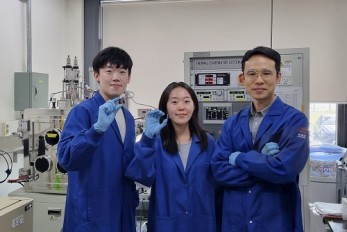
Metasurface technology is an advanced optical technology that is thinner, lighter, and capable of precisely controlling light through nanometer-sized artificial structures compared to conventional technologies. KAIST researchers have overcome the limitations of existing metasurface technologies and successfully designed a Janus metasurface capable of perfectly controlling asymmetric light transmission. By applying this technology, they also proposed an innovative method to significantly enhance security by only decoding information under specific conditions. KAIST (represented by President Kwang Hyung Lee) announced on the 15th of October that a research team led by Professor Jonghwa Shin from the Department of Materials Science and Engineering had developed a Janus metasurface capable of perfectly controlling asymmetric light transmission. Asymmetric properties, which react differently depending on the direction, play a crucial role in various fields of science and engineering. The Janus metasurface developed by the research team implements an optical system capable of performing different functions in both directions. Like the Roman god Janus with two faces, this metasurface shows entirely different optical responses depending on the direction of incoming light, effectively operating two independent optical systems with a single device (for example, a metasurface that acts as a magnifying lens in one direction and as a polarized camera in the other). In other words, by using this technology, it's possible to operate two different optical systems (e.g., a lens and a hologram) depending on the direction of the light. This achievement addresses a challenge that existing metasurface technologies had not resolved. Conventional metasurface technology had limitations in selectively controlling the three properties of light—intensity, phase, and polarization—based on the direction of incidence. The research team proposed a solution based on mathematical and physical principles, and succeeded in experimentally implementing different vector holograms in both directions. Through this achievement, they showcased a complete asymmetric light transmission control technology. < Figure 1. Schematics of a device featuring asymmetric transmission. a) Device operating as a magnifying lens for back-side illumination. b) Device operating as a polarization camera for front-side illumination. > Additionally, the research team developed a new optical encryption technology based on this metasurface technology. By using the Janus metasurface, they implemented a vector hologram that generates different images depending on the direction and polarization state of incoming light, showcasing an optical encryption system that significantly enhances security by allowing information to be decoded only under specific conditions. This technology is expected to serve as a next-generation security solution, applicable in various fields such as quantum communication and secure data transmission. Furthermore, the ultra-thin structure of the metasurface is expected to significantly reduce the volume and weight of traditional optical devices, contributing greatly to the miniaturization and lightweight design of next-generation devices. < Figure 2. Experimental demonstration of Janus vectorial holograms. With front illuminations, vector images of the butterfly and the grasshopper are created, and with the back-side illuminations, vector images of the ladybug and the beetle are created. > Professor Jonghwa Shin from the Department of Materials Science and Engineering at KAIST stated, "This research has enabled the complete asymmetric transmission control of light’s intensity, phase, and polarization, which has been a long-standing challenge in optics. It has opened up the possibility of developing various applied optical devices." He added, "We plan to continue developing optical devices that can be applied to various fields such as augmented reality (AR), holographic displays, and LiDAR systems for autonomous vehicles, utilizing the full potential of metasurface technology." This research, in which Hyeonhee Kim (a doctoral student in the Department of Materials Science and Engineering at KAIST) and Joonkyo Jung participated as co-first authors, was published online in the international journal Advanced Materials and is scheduled to be published in the October 31 issue. (Title of the paper: "Bidirectional Vectorial Holography Using Bi-Layer Metasurfaces and Its Application to Optical Encryption") The research was supported by the Nano Materials Technology Development Program and the Mid-Career Researcher Program of the National Research Foundation of Korea.
-
Hyeong-Seok Ko & Hyeon-Ho Yang (Advisor: Prof. Ja..
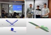
Hyeong-Seok Ko and Hyun-Ho Yang, from KAIST AE’s Smart Structures and Hardware Systems Lab (Advisor: Jae-Hung Han), achieved first place in the "2024 RecurDyn Simulation Competition" hosted by FunctionBay, Inc. Competing against 42 teams, they secured the Gold Award (1st) for the second consecutive year, following from last year. Their presentation topic was "Integrated Simulation Program for Bird-Inspired Flapping-Wing Air Vehicles", in which they developed a fluid-structure interaction analysis program for ornithopters in forward flight by integrating RecurDyn's multi-flexible-body dynamics solver and the modified unsteady vortex lattice method. RecurDyn is a comprehensive CAE dynamics analysis software that offers various functions such as control, fatigue analysis, and optimization, with ulti-flexible-body dynamics at its core, spanning across different fields.
-
KAIST Develops Stretchable Displays Featuring 25% ..
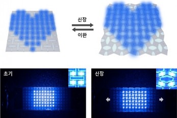
Stretchable displays, praised for their spatial efficiency, design flexibility, and human-like flexibility, are seen as the next generation of display technology. A team of Korean researchers has developed a stretchable display that can expand by 25% while maintaining clear image quality without distortion. It can also stretch and contract up to 5,000 times at 15% expansion without any performance degradation, making it the first deformation-free stretchable display with a negative Poisson's ratio* developed in Korea. *Poisson’s ratio of -1: A ratio where both width and length stretch equally, expressed as a negative value. A positive Poisson's ratio represents the ratio where horizontal stretching leads to vertical contraction, which is the case for most materials. KAIST (represented by President Kwang-Hyung Lee) announced on the 20th of August that a research team led by Professor Byeong-Soo Bae of the Department of Materials Science and Engineering (Director of the Wearable Platform Materials Technology Center) , in collaboration with the Korea Institute of Machinery & Materials (President Seoghyeon Ryu), successfully developed a stretchable display substrate that suppresses image distortion through omnidirectional stretchability. Currently, most stretchable displays are made with highly elastic elastomer* materials, but these materials possess a positive Poisson's ratio, causing unavoidable image distortion when the display is stretched. *Elastomer: A polymer with elasticity similar to rubber. To address this, the introduction of auxetic* meta-structures has been gaining attention. Unlike conventional materials, auxetic structures have a unique 'negative Poisson's ratio,' expanding in all directions when stretched in just one direction. However, traditional auxetic structures contain many empty spaces, limiting their stability and usability in display substrates. *Auxetic structure: A special geometric structure that exhibits a negative Poisson's ratio. To tackle the issue of image distortion, Professor Bae's research team developed a method to create a seamless surface for the auxetic meta-structure, achieving the ideal negative Poisson's ratio of -1 and overcoming the biggest challenge in auxetic meta-structures. To overcome the second issue of elastic modulus*, the team inserted a textile made of glass fiber bundles with a diameter of just 25 micrometers (a quarter of the thickness of human hair) into the elastomer material. They then filled the empty spaces with the same elastomer, creating a flat and stable integrated film without gaps. *Elastic Modulus: The ratio that indicates the extent of deformation when force is applied to a material. A higher elastic modulus means that the material is less likely to deform under force. The research team theoretically identified that the difference in elasticity between the auxetic structure and the elastomer material directly influences the negative Poisson's ratio and successfully achieved an elasticity difference of over 230,000 times, producing a film with a Poisson's ratio of -1, the theoretical limit. < Figure 2. Deformation of S-AUX film. a) Configurations and visualized principal strain distribution of the optimized S-AUX film at various strain rates. b) Biaxial stretching image. While pristine elastomer shrinks in the directions that were not stretched, S-AUX film developed in this study expands in all directions simultaneously while maintaining its original shape. > Professor Byeong-Soo Bae, who led the study, explained, "Preventing image distortion using auxetic structures in stretchable displays is a core technology, but it has faced challenges due to the many empty spaces in the surface, making it difficult to use as a substrate. This research outcome is expected to significantly accelerate commercialization through high-resolution, distortion-free stretchable display applications that utilize the entire surface." This study, co-authored by Dr. Yung Lee from KAIST’s Department of Materials Science and Engineering and Dr. Bongkyun Jang from the Korea Institute of Machinery & Materials, was published on August 20th in the international journal Nature Communications under the title "A seamless auxetic substrate with a negative Poisson's ratio of –1". The research was supported by the Wearable Platform Materials Technology Center at KAIST, the Korea Institute of Machinery & Materials, and LG Display. < Figure 3. Structural configuration of the distortion-free display components on the S-AUX film and a contour image of a micro-LED chip transferred onto the S-AUX film. > < Figure 4. Schematic illustrations and photographic images of the S-AUX film-based image: distortion-free display in its stretched state and released state. >

291 Daehak-ro, Yuseong-gu, Daejeon, Korea 34141
KAIST College of Engineering
T.+82-42-350-2114
F.+82-42-350-2210 (2220)
ⓒ KAIST College of Engineering. All rights reserved.