


Faculty News
-

KAIST Finds Clue to Solving the “Electrical Bottle..
< Figure 1. (From left to right) KAIST Professor Kibum Kang, Dr. Minseung Gyeon, Ph.D. candidate Yeongyu Kim, and Professor Seungbum Hong; and, in the circles from left, Sungkyunkwan University Ph.D. candidate Ji Hoon Hong and Professor Sung Beom Cho. > When the pathways through which electricity flows inside a semiconductor become blocked, device performance declines and power loss increases. A Korean research team has developed a new structure that could resolve this “electrical bottleneck” and, for the first time, directly confirmed that electric charges flow continuously without interruption. This achievement is expected to become a key technology for improving the performance and power efficiency of future semiconductors, including AI semiconductors and ultra-low-power semiconductors. KAIST announced on July 13 that a research team led by Professor Seungbum Hong from the Department of Materials Science and Engineering, in collaboration with Professor Kibum Kang from the Department of Materials Science and Engineering at KAIST and Professor Sung Beom Cho’s research team at Sungkyunkwan University, has realized a new structure in which electricity flows without obstruction in a two-dimensional material—an ultrathin material only one or two atomic layers thick—that is attracting attention for next-generation semiconductor devices. The team also developed an analytical platform capable of directly observing this charge transport at the nanometer scale. In semiconductors, contact resistance, which arises at the interface where a metal electrode meets a semiconductor, degrades performance and causes power loss. Especially as semiconductors continue to scale down, the influence of contact resistance becomes even greater, making it one of the most challenging technical bottlenecks in developing next-generation semiconductors. < Figure 2. (AI-generated image) Conceptual diagram of the research explained by KAIST’s mascot character (Nubzuki) > Instead of attaching a metal electrode on top of a semiconductor as in conventional approaches, the research team continuously formed semi-metallic and semiconducting regions within a single two-dimensional m aterial. By creating a structure in which the two regions are naturally connected within the same material, the team demonstrated for the first time that current can flow across the boundary without being blocked. Specifically, the team continuously implemented a semi-metallic region and a semiconducting region within a single thin film of platinum diselenide (PtSe₂), an atomically thin two-dimensional material. By realizing a monolithic structure, in which a single material is formed continuously without interruption, the team proposed a new structure that allows current to flow across the boundary without obstruction. Using Atomic Force Microscopy (AFM), a microscope that uses a probe to measure surface and electrical properties down to the atomic level, the team directly visualized charge transport inside the thin film at the nanometer scale. As a result, the team confirmed for the first time that, when current moved from the semi-metallic region to the semiconducting region, the flow continued naturally without an “electrical bottleneck,” such as a blockage or bending of the current path. This is the first experimental demonstration that a monolithic interface does not interfere with current flow. Furthermore, the team verified device operation by applying an electric field to the semiconducting region. The results confirmed that current flow can be stably controlled in a metal–semiconductor junction structure, demonstrating the potential of the structure for next-generation electronic devices. < Figure 3. The Research Infographic > This study presents a source technology that can dramatically reduce contact resistance in next-generation semiconductor devices based on two-dimensional materials. It is expected to be widely applicable to the development of future semiconductor technologies, including AI semiconductors, ultra-low-power semiconductors, and next-generation logic semiconductors. The study was co-first-authored by Yeongyu Kim, a Ph.D. candidate and Dr. Minseung Gyeon from the Department of Materials Science and Engineering at KAIST; and Ji Hoon Hong, a Ph.D. candidate at Sungkyunkwan University. The work was published in the July 2026 issue of Matter, an international journal in the field of materials science. ※ Paper title: Nanoscale imaging of charge transport across the semimetal-semiconductor interface in monolithic platinum diselenide DOI:https://doi.org/10.1016/j.matt.2026.102873 This research was supported by the STEAM Research Program and the Nanomaterials Technology Development Program of the Ministry of Science and ICT and the National Research Foundation of Korea.
-

KAIST Develops AI Technology to Detect Early Warni..
< The Research Team Members From left, Professor Jo woon Chong from Sungkyunkwan University, Professor Lisa Lim from KAIST, Professor Kyung-Hee Cho from Korea University Anam Hospital, and, bottom row, Dr. Jeongyeop Baek of the KAIST Institute for Applied Science. > Cerebrovascular disease can lead to serious aftereffects if treatment is delayed, but it is difficult to detect before symptoms appear. KAIST researchers have developed an AI technology that analyzes real-life daily activity and environmental data from older adults to identify digital behavioral markers of cerebrovascular disease risk based on subtle changes at home. KAIST (President Choongsik Bae) announced on the 12th of July that a research team led by Professor Lisa Lim from the Department of Civil and Environmental Engineering, in collaboration with Professor Jo Woon Chong from the School of Electronic and Electrical Engineering at Sungkyunkwan University (President Ji-Beom Yoo) and Professor Kyung-Hee Cho from the Department of Neurology at Korea University Anam Hospital (President Dongwon Kim), has developed an AI framework that uses long-term lifelog data collected in the homes of older adults to identify the prodromal phase of cerebrovascular disease and assess imminent diagnostic risk. The study was based on lifelog data from 1,224 older adults collected by LivOn Care Co., Ltd. in real residential environments. The research team analyzed a total of 13,362 two-week lifelog samples, demonstrating the possibility of detecting early warning signs through subtle changes in daily life, rather than relying only on the conventional approach of treating the disease after it has already occurred. The research team developed AI technology that identifies cerebrovascular disease risk stages by analyzing daily activity, sleep, circadian rhythm, and indoor environmental information, together with age and chronic disease data. This shows that changes in everyday living patterns, which are difficult to capture through hospital examinations alone, can serve as important clues for detecting early risk signals of cerebrovascular disease. The team also succeeded in assessing whether a cerebrovascular disease diagnosis was approaching by analyzing changes in lifestyle patterns over time. When lifelog data from within four weeks before diagnosis were classified as the “imminent diagnostic risk period” and data from 12 weeks before diagnosis were classified as the “non-imminent period,” the AI distinguished between the two periods with a high accuracy of 96.53%. This result suggests that even before a hospital visit, small changes in daily life may help identify whether the risk of cerebrovascular disease has increased. < Figure1. A Research Image: Using AI to analyze activity, sleep, daily-rhythm, and indoor environmental data collected through contactless sensors in older adults’ homes, the study identifies a “pre-diagnosis risk group” between healthy and diagnosed groups and evaluates “imminent risk” as the time of diagnosis approaches. > Another key feature of this study is that the AI does not simply determine whether a risk exist, but also applies explainable AI to identify the lifestyle patterns and environmental factors behind its judgment. The analysis showed that older adults in the prodromal phase of cerebrovascular disease tended to show frequent continuous activity between 10 p.m. and 2 a.m., a time when the body would normally be preparing for sleep. In other words, irregular daily rhythms, such as delayed sleep onset and a reduced distinction between day and night activity, were closely associated with prodromal signals of cerebrovascular disease. The researchers also found that as the time of diagnosis approached, the frequency of continuous activity during the evening period from 6 p.m. to 10 p.m. noticeably decreased, while inactive time increased. Low indoor humidity, indicating a dry indoor environment, also emerged as an important factor in identifying an imminent diagnostic risk. The research team expects this technology to be used as a digital healthcare tool that can objectively monitor the health status of older adults who may have difficulty clearly describing their own condition, while providing useful early warning indicators to medical professionals and caregivers. However, the team explained that this study does not predict the exact onset of cerebrovascular disease or replace clinical diagnosis. Rather, it is a supportive technology intended to aid prevention and early medical consultation, and prospective validation in larger patient groups will be necessary before actual clinical application. Professor Lisa Lim said, “The key point of this study is not that AI should replace a hospital diagnosis, but that it can first detect risk signals in small lifestyle changes at home and help connect patients to medical care at the right time,” adding, “We expect this technology to contribute to a shift from a healthcare system that treats disease after it occurs to one that supports prevention and early intervention.” This study, with KAIST Dr. Jeongyeop Baek as the first author, was published on June 2 in npj Digital Medicine, a leading international journal in digital healthcare published by Nature Portfolio, with an impact factor of 15.1 and ranked in the top 0.3% of JCR journals. ※ Paper title: AI home monitoring for behavioral markers of cerebrovascular disease DOI: https://doi.org/10.1038/s41746-026-02836-7 This work was also supported by the National Research Foundation (NRF) grant funded by the Korea government (Ministry of Science and ICT) (RS-2025-16068234).
-

KAIST Automates the Search for “Dream Semiconducto..
< Research team members: From left, Professor Jimin Kwon, Dr. Haksoon Jung, and Dr. Yongwoo Lee of KAIST > The era of researchers manually searching for two-dimensional semiconductors, which are drawing attention as next-generation AI semiconductors, is coming to an end. KAIST researchers have automated semiconductor screening and device fabrication, analyzed thousands of devices, and revealed the relationship between thickness and performance that had long been difficult to identify. This achievement is expected to shift next-generation semiconductor research toward a data-driven approach and accelerate the commercialization of AI semiconductors and ultra-low-power semiconductors. KAIST (President Choongsik Bae) announced on the 9th that a research team led by Professor Jimin Kwon of the School of Electrical Engineering and the Department of AI System has developed a technology that automatically identifies two-dimensional semiconductors from optical microscope images alone and connects the process to transistor fabrication, through joint research with UNIST, Hanbat National University, Hanyang University, and Washington University in St. Louis in the United States. < Figure1. Optical-image-based framework for MoS₂ flake identification and device fabrication > Two-dimensional semiconductors are ultrathin semiconductors only a few atomic layers thick. They are called “dream semiconductors” because they can enable smaller semiconductors that consume less electricity than conventional silicon semiconductors. Today’s silicon semiconductors are approaching physical limits, as continued miniaturization of circuits leads to greater power loss and heat generation. Two-dimensional semiconductors, which are attracting attention as next-generation materials to overcome these limits, are expected to be used in a wide range of future technologies, including AI semiconductors, smartphones, data centers, wearable devices, foldable or stretchable electronics, and ultra-small medical sensors. However, in two-dimensional semiconductors made through solution processing, the position, size, and thickness of each small semiconductor flake all differ, requiring researchers to find the desired samples one by one under a microscope. They then had to manually design electrodes according to the identified positions, requiring substantial time and effort, and making it practically difficult to analyze thousands or more devices at once. The research team used molybdenum disulfide (MoS₂), a representative two-dimensional semiconductor material. By using the fact that the RGB red, green, and blue brightness values seen under a microscope change depending on thickness, the team enabled a computer to automatically identify the desired semiconductor and automatically design the electrodes. Verification using atomic force microscopy (AFM) confirmed that even subtle thickness differences of three to eight layers could be accurately distinguished. Through this approach, the team successfully selected suitable samples automatically from more than 120,000 semiconductor flakes and fabricated and analyzed 1,615 transistors. The large-scale analysis also produced meaningful results. The team statistically clarified for the first time that as the semiconductor becomes thicker, current flows more easily, but the ability to switch electricity on and off actually decreases. This characteristic had been difficult to confirm previously because only a small number of samples could be analyzed, but the team revealed it through large-scale data. < Figure 2. Verification of MoS₂ layer number based on the selection factor (S) and RG-channel brightness clustering > The greatest significance of this study is that it did not simply automate the fabrication process, but transformed two-dimensional semiconductor research, which had relied on human experience, into data-driven research. Going forward, the technology is expected to enable researchers to fabricate and analyze more semiconductors more quickly, identify high-performance materials, and ultimately expand into research in which AI designs new semiconductors. This study was conducted with Professor Jimin Kwon, Dr. Haksoon Jung, and Dr. Yongwoo Lee of KAIST as co-corresponding authors, and Sanghyun Lee of UNIST as the first author. The research results were published on April 3 in Advanced Functional Materials, a leading international journal in materials science, and were also selected as an Inside Back Cover article in the field of 2D Materials & Electronics. ※ Paper title: Statistically Resolving Thickness-Dependent Electrical Characteristics in Multilayer-MoS₂ Transistors, DOI: 10.1002/adfm.202532204 ※ Author information: Professor Jimin Kwon (KAIST, corresponding author), Dr. Haksoon Jung (KAIST, corresponding author), Dr. Yongwoo Lee (KAIST, corresponding author), Sanghyun Lee (UNIST, first author), and participating researchers from partner institutions: Sumin Hong (UNIST), Minho Park (UNIST), Professor Seongju Kim (Hanbat National University), Professor Sang-Hoon Baek (Hanyang University), Professor Joonki Suh (KAIST), Seonguk Yang (KAIST), Professor Sang-Hoon Bae (Washington University in St. Louis), and Dr. Chang-Soo Lee (TDS) This research was supported by the Individual Basic Research Program of the National Research Foundation of Korea (NRF), funded by the Ministry of Science and ICT (MSIT), and by the Advanced Strategic Industry Super-Gap Technology Development Program of the Korea Planning & Evaluation Institute of Industrial Technology (KEIT), funded by the Ministry of Trade, Industry and Energy (MOTIE).
-

KAIST Develops Core Display Technology That Preven..
< Demonstration image of the proposed stretchable display technology (Concept image, AI-generated) > Beyond bendable and foldable displays, the era of stretchable displays, whose screens can expand freely like rubber, is now emerging. KAIST researchers have developed a core technology that allows text, images, and other on-screen information to retain their original shape even when the screen is stretched by up to 15%. The achievement is expected to help solve the problem of image distortion and accelerate the commercialization of next-generation high-quality stretchable displays. KAIST (President Choongsik Bae) announced on the July 8 that a research team led by Professor Seunghyup Yoo of the School of Electrical Engineering, in collaboration with Professor Hanul Moon’s team at Dong-A University (President Hae Woo Lee), has successfully implemented an auxetic-based stretchable display platform. Auxetic structures expand in both width and length when pulled, allowing the display to stretch uniformly at the same ratio in all directions without distorting the image on the screen. Conventional stretchable displays are generally made by forming light-emitting devices on a stretchable substrate, which serves as the base layer of the display. However, when such a substrate is stretched in one direction, it tends to shrink in the opposite direction, causing letters and images on the screen to become flattened or distorted. Auxetic structures have been used to address this problem, but most previous approaches were limited to maintaining the overall horizontal-to-vertical ratio of the screen, while the letters and images within the screen still remained vulnerable to distortion. Instead of bonding the auxetic structure and the stretchable substrate across the entire surface, as in conventional methods, the research team proposed a new design approach that uses computational analysis to selectively connect only the necessary points that ensure isotropic expansion throughout the substrate. In the conventional approach, the twisting deformation that occurs as the auxetic structure stretches is directly transferred to the substrate, distorting the image inside the screen. In contrast, the platform developed by the research team was designed so that each region moves evenly outward from its original position. This allows not only the entire screen but also small areas such as letters and images to expand together while maintaining their original shapes. < Figure1. Image distortion limitations of conventional stretchable displays (Upper row) and the auxetic-based stretchable display design proposed in this study, including its selective bonding strategy. > The research team verified the platform’s performance by repeatedly stretching a substrate patterned with letters and images in both the horizontal and vertical directions. In the conventional method, the patterns underwent local deformation, whereas in the new platform, the shapes of the letters and images remained intact. This demonstrates that not only the whole screen but also fine images on-screen can expand uniformly without distortion. The team also integrated an LED array, a structure in which multiple LEDs are arranged at regular intervals, onto the platform to verify its performance as an working stretchable display. Even when stretched by up to 15% in both the horizontal and vertical directions, stable electrical operation and the screen brightness were maintained. After repeated stretching to 15%, the decrease in brightness remained below 2%, confirming the platform’s potential for practical display applications. < Figure2. Demonstration of distortion-free characteristics of the proposed auxetic-based stretchable display (right) in comparison to those of conventional, fully-bonded auxetic-based stretchable displays(left) > This technology is expected to serve as a core platform for next-generation electronics with freely changeable shapes, including wearable electronic devices, electronic skin, or e-skin, which refers to electronic devices that stretch like skin while sensing and displaying information, medical biosensors, soft robots, and curved displays for automobiles and aircraft. Professor Seunghyup Yoo of KAIST said, “For stretchable displays to be used as actual information display devices, they must not only stretch well, but also preserve on-screen information accurately during stretching,” adding, “This platform enables uniform expansion from small areas of the screen to the entire display, and will serve as a key foundational technology for accelerating the commercialization of high-quality stretchable displays.” This study was led by KAIST Dr. Su-Bon Kim and Dr. Junho Kim as co-first authors, with Professor Hanul Moon of Dong-A University and Professor Seunghyup Yoo of KAIST as co-corresponding authors. The research was published in the international journal Nature Communications on June 10. ※ Paper title: Hybrid auxetic metamaterial platforms enabling multiscale isotropic expansion for distortion-free stretchable displays, DOI: 10.1038/s41467-026-74141-6 This research was supported by the National Research Foundation of Korea (NRF) Mid-Career Researcher Program, the Future Display Strategic Research Laboratory Program, the Korea Planning & Evaluation Institute of Industrial Technology (KEIT), and the Korea Institute for Advancement of Technology (KIAT) HRD Program.
-

KAIST Identifies the “Hidden Energy Cost” of AI Ag..
< Byeongjun Shin, master’s student; Jinha Chung, M.S./Ph.D. integrated student; Jiin Kim, Ph.D. student; and, at top, Professor Minsoo Rhu of KAIST. > As the era of AI agents—systems that can reason and act autonomously—begins, the power consumption of data centers is emerging as a critical challenge. A KAIST research team has, for the first time, analyzed the computational cost and energy consumption of AI agents, finding that they can consume up to 136.5 times energy per query than conventional generative AI. The study shows that competitiveness in the AI era is expanding beyond model performance to include the efficiency of data centers and power infrastructure. KAIST announced that a research team led by Professor Minsoo Rhu of the School of Electrical Engineering has systematically analyzed, for the first time, how much computational resources and power AI agents require in real-world service environments. Large language model (LLMs) powered applications such as ChatGPT have rapidly evolved beyond simply answering questions. They are now developing into AI agents: next-generation AI systems that can plan, use external tools such as web search, calculators, and code execution environments, and solve complex tasks by coordinating multiple steps on their own. Although AI agents are increasingly being adopted in areas such as software development, research, and workplace automation, little has been known about the amount of electricity and operational cost required to run them in practice. The research team defined AI agents not merely as software programs, but as a new type of workload that must be continuously processed by data-center servers and graphics processing units, or GPUs—high-performance chips used for large-scale AI computation. The team then analyzed the computational load and energy consumption incurred during actual AI agent execution. The analysis found that AI agents perform, far higher volumes of LLM invocations than conventional chain-of-thought reasoning. Chain-of-thought, or CoT, refers to a method in which an AI model breaks down its reasoning process step by step to reach an answer, while an LLM invocation refers to each computational request made to a language model to generate a new judgment or response. < Figure 1. Key Characteristics of AI Agents and Their Infrastructure Implications > Because AI agents repeatedly call language models during execution, their response latency also increases significantly. The team found that response time can increase by up to 153.7 times, while GPUs remain idle for as much as 54.5 percent of the total execution time as external tools perform their tasks. In other words, as AI systems take on more complex tasks, a new form of inefficiency emerges in which expensive GPUs cannot be fully utilized. The research team also analyzed the power consumption of AI agents at data-center scale. An AI agent using a 70-billion-parameter LLM—a scale comparable to current commercial AI services—consumed an average of 348.41 watt-hours per query. This is 136.5 times higher than the energy consumed by a conventional generative AI system performing simple question answering. In addition, the team projected a future scenario in which 13.7 billion AI agent requests are generated per day — a volume equivalent to current Google search traffic. Under this scenario, data-center power demand would reach approximately 198.9 gigawatts, a level far exceeding the scale of AI data centers currently under development (which are in the range of a few gigawatts) and equivalent to roughly half of the average power consumption of the United States. This study demonstrates that the focus of competition in the AI era is shifting from “smarter AI” to “optimally efficient AI.” Going forward, it will be essential not only to advance AI models, but also to jointly optimize AI semiconductors, data centers, and power infrastructure through co-design. Such an approach is expected to become a key strategy for reducing the operating cost of AI services and building sustainable AI infrastructure. “This study is the first to quantitatively show not only how AI is becoming more intelligent, but also how much electricity and cost are required to implement and sustain that intelligence,” said Professor Rhu. “As AI agents become widespread, it will become increasingly important to take an integrated co-design approach that optimizes not only AI data-center infrastructure, but also AI agent models and power infrastructure.” He added, “Research and investment in this direction will be essential to dramatically reduce the cost for end users to access AI services while building sustainable AI infrastructure.” The study was conducted with Jiin Kim, a Ph.D. student in the KAIST School of Electrical Engineering, as the first author. The paper was presented in February at the 32nd IEEE International Symposium on High-Performance Computer Architecture, or HPCA, one of the most prestigious international conferences in computer system design. The research team has also released the AI agent implementations and benchmarks used in the paper as open source to support follow-up studies by researchers worldwide. Paper title: “The Cost of Dynamic Reasoning: Demystifying AI Agents and Test-Time Scaling from an AI Infrastructure Perspective” Open-source repository: 10.1109/HPCA68181.2026.11408569 This research was supported by the Institute of Information & Communications Technology Planning & Evaluation (IITP) through the SW Starlab program, the K-Cloud Technology Development Program using AI semiconductors, and the Leading Technology Development Program for Advancing AI-Semiconductor-Based Data Centers, as well as by the Samsung Electronics Future Technology Incubation Center.
-

Crude Oil Separates Without Boiling: KAIST and Ge..
< Simple synthetic membrane supports yield surprisingly selective separation of real crude oils at steady state. Credit: KAIST > An international research team led by KAIST has developed a membrane technology that could significantly reduce the energy required for crude oil refining by replacing part of the century-old distillation process. KAIST(President Kwang Hyung Lee) announced that a team led by Professor Dong-Yeun Koh of KAIST, in collaboration with Professor Ryan Lively's group at Georgia Tech, demonstrated a simple and inexpensive membrane capable of separating crude oil at room temperature without heating. The research was published in Nature, one of the world's leading scientific journals. Crude oil underpins modern life by providing not only transportation fuels but also essential feedstocks for plastics, packaging materials, textiles, and countless consumer products. Because the cost of refining directly influences the price of these products, technologies that reduce refining energy consumption can generate substantial economic and environmental benefits. Traditionally, refineries separate crude oil through distillation, a process that heats crude oil above 350 °C to vaporize it and then cools the vapor to recover different fractions. Globally, crude oil distillation consumes approximately 1,100 terawatt-hours (TWh) of energy each year—equivalent to the annual output of about 130 nuclear power plants, each at gigawatt scale, operating continuously. As a result, distillation remains one of the largest sources of energy consumption and greenhouse gas emissions in the refining industry. At the same time, increasing cost pressures in global petrochemical markets have intensified the need for more energy-efficient separation technologies. Membrane-based crude oil fractionations have attracted increasing attention as a potential alternative. However, conventional wisdom has held that molecularly precise separation requires an ultrathin selective layer coated onto the membrane surface. While effective, such coatings increase manufacturing costs and are prone to defects when scaled to large areas, limiting industrial deployment. To overcome this challenge, the researchers took a radically different approach. Instead of relying on a specialized coating, they passed crude oil directly through a bare porous polyacrylonitrile (PAN) membrane—a chemically stable and inexpensive polymer commonly used as a support material in industrial membranes. As crude oil permeated through the membrane, heavy hydrocarbons selectively deposited on the pore walls, gradually narrowing the pores and creating self-assembled separation channels smaller than 2 nanometers. Rather than relying on a specially engineered coating, the crude oil itself created the nanoscale pathways needed for precise molecular separation. Through these self-formed channels, lighter fractions such as naphtha, gasoline, and kerosene permeated rapidly, while heavier components were effectively retained. In a surprising reversal, membrane fouling—normally regarded as a performance-degrading phenomenon—became the very mechanism that enabled highly selective separation. The bare PAN membrane delivered crude oil permeation rates approximately 23 times higher than those of previously reported state-of-the-art crude oil membranes while maintaining stable performance for 28 consecutive days. Professor Ryan Lively (Georgia Tech) commented “one of the key challenges facing membrane systems for crude oil separation was the low productivities of the membrane units – the PAN membranes with their surprising separation mechanism – dramatically increase the productivity of the membrane unit, to the point where industry should seriously consider adopting the technology.” Importantly, the technology can be integrated into existing refinery infrastructure as a modular filtration unit, avoiding major equipment replacement and reducing barriers to industrial adoption. Process simulations showed that using the membrane as a pretreatment step before conventional distillation could reduce energy consumption by 31.6%, carbon dioxide emissions by 37.6%, cooling water usage by 20.7%, and operating costs by 36%. If adopted throughout Korea's refining and petrochemical sector, the technology could reduce greenhouse-gas emissions by approximately 10 million tonnes annually—equivalent to the emissions of roughly four million internal combustion vehicles. Beyond crude oil refining, the membrane platform could be applied to a broad range of chemical separation processes, including the purification of pyrolysis oil derived from waste plastics, the recovery of solvents used in battery manufacturing, pharmaceutical purification, and biofuel production. The researchers believe the technology could serve as a versatile platform for next-generation molecular separations across multiple industries. Professor Dong-Yeun Koh of KAIST said, “This study reveals a new scientific principle in which a membrane interacts with a complex mixture and spontaneously forms its own separation channels. Working with real crude oil supplied by HD Hyundai Oilbank allowed us to validate the technology under conditions relevant to industrial operation.” Professor Jae W. Lee of KAIST, a co-corresponding author of the study, added, “By advancing large-area membrane modularization and long-term operational reliability, we hope to broaden the adoption of membrane-based processes throughout the refining and petrochemical industries.” Dr. Jihoon Choi and Dr. Hyeokjun Seo of KAIST, the study’s co-first authors, said, “Our goal is to precisely control this spontaneous pore-constriction phenomenon and develop it into a membrane platform applicable to the entire refining process. We also aim to expand the technology to plastic recycling, biofuel purification, and other sustainable chemical processes that support carbon neutrality.” The study was co-first-authored by Dr. Jihoon Choi and Dr. Hyeokjun Seo of KAIST and was published online in Nature on June 24, 2026. Paper Title: Crude Oil Fractionation by Means of Mesoporous Polyacrylonitrile Membranes DOI 10.1038/s41586-026-10677-3 https://www.nature.com/articles/s41586-026-10677-3 This research was supported by the Ministry of Science and ICT of Korea through the Basic Research Program for Outstanding Early-Career Researchers and the Engineering Research Center (ERC) Program.
-
KAIST Teams Win Both International Challenges at I..
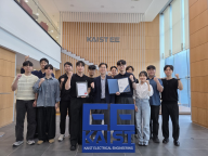
< From left: the ACDC-K Team, Prof. Hyun Myung, and the Curaytor Team. > Two research teams from KAIST have claimed first place in international challenge competitions held at the world’s premier robotics and computer vision conferences. KAIST (President Kwang-Hyung Lee) announced that the ACDC-K Team and the Curaytor Team, both from the laboratory of Prof. Hyun Myung in the School of Electrical Engineering, won first place in international challenge competitions held in conjunction with the IEEE International Conference on Robotics and Automation (ICRA 2026) and the IEEE/CVF Conference on Computer Vision and Pattern Recognition (CVPR 2026), respectively. The achievement highlights the global competitiveness of KAIST’s robotic perception and spatial intelligence technologies, with two teams from the same laboratory securing victories in leading international competitions across distinct research fields. The ACDC-K Team won first place among more than 60 participating teams in the SLAM (Simultaneous Localization And Mapping) category of the Hilti×Trimble SLAM Challenge 2026, held during the Open Challenges in Robotics for Asset Inspection (OCRAIM) Workshop at ICRA 2026 in Vienna, Austria, from June 1 to 5. < Example of SLAM (Simultaneous Localization and Mapping) results generated by the ACDC-K Team’s proposed technology in a 40 m × 30 m construction environment. > Jointly organized by Hilti, Trimble, and the University of Oxford, the challenge evaluates robotic localization and mapping performance using sensor data collected from real construction sites. Participants were required to address practical challenges frequently encountered in construction environments, including non-overlapping front and rear fisheye camera configurations, low-texture indoor scenes, and rapid camera motion. To tackle these challenges, the ACDC-K Team developed a robust visual-inertial SLAM system that fuses front and rear fisheye camera data with inertial measurements. By integrating feature-point and feature-line observations with adaptive constraints and correction mechanisms, the team achieved highly reliable localization and mapping performance in complex construction environments. Meanwhile, the Curaytor Team won first place among eight participating teams in the Nothing Stands Still (NSS) Challenge 2026, held during the Computer Vision for the Built World (CV4AEC) Workshop at CVPR 2026 in Denver, Colorado, from June 3 to 7. < Example of multiway registration results generated by the Curaytor Team’s proposed technology in a large-scale environment covering approximately 4,960 m² > Jointly organized by Stanford University, ETH Zurich, and Oregon State University, the NSS Challenge evaluates 3D point cloud registration technologies for construction and industrial environments that evolve over time. The Curaytor Team developed a novel multi-registration framework capable of aligning multiple LiDAR scans collected across different times and locations. The framework integrates feature extraction, correspondence estimation, robust global registration, registration confidence assessment, and change-aware refinement techniques. As a result, the team achieved highly accurate registration performance even in environments containing structural changes and dynamic objects. < . Curaytor Team receiving the award. Kim Daebeom (Team Leader, Ph.D. candidate). > “This achievement demonstrates the robustness of our visual-inertial SLAM and 3D LiDAR registration technologies in complex and constantly changing real-world environments,” said Prof. Hyun Myung. “It is particularly meaningful that our students secured first-place finishes in highly competitive international challenges hosted at two of the world’s most prestigious conferences in robotics and computer vision.” Prof. Hyun Myung’s laboratory has consistently demonstrated excellence in spatial intelligence research. The laboratory previously won first place in the LiDAR track and ranked first among academic teams in the vision track of the Hilti SLAM Challenge in 2023. In addition, the Curaytor Team successfully defended its title in the NSS Challenge, securing back-to-back championships in 2025 and 2026. < . ACDC-K Team at the award ceremony. From left: Jinwoo Jeon (Ph.D. candidate, Team Leader) and Prof. Hyun Myung. >
-

KAIST Develops Next-Generation Self-Powered Wearab..
< Photo of the KAIST research team. From left to right: Prof. Miso Kim, JungHun Park (Ph.D. student), Yong Jun Choi (Research Associate; first author), Jisoo Nam (Ph.D. student), and Prof. Gi-Dong Sim > Wearable medical devices that monitor heart rate, respiration, and joint movements for long periods without battery concerns, electronic skins that sense external stimuli like human skin, and soft robots made of flexible materials that move freely have all come one step closer to reality. KAIST researchers have developed a self-powered sensor (a sensor that generates electricity on its own without a battery) that can stretch up to 668% while producing stable electrical signals. KAIST announced on June 18th that a research team led by Professor Miso Kim from the Department of Mechanical Engineering has overcome the durability limitations of conventional piezoelectric fiber sensors (fiber-type sensors that convert pressure or movement into electrical signals) and successfully developed a highly stretchable piezoelectric fiber sensor that operates stably even under repeated deformation. < Conceptual illustration of a self-powered piezoelectric fiber coil sensor (AI-generated) > The core material of the sensor, piezoelectric polymer, is a polymeric material that generates electricity when subjected to mechanical force. Although its lightweight and flexible nature makes it suitable for skin-attachable wearable sensors, conventional piezoelectric fiber sensors suffered from signal degradation during repeated stretching or bending, as the electrode layer collecting electrical signals and the piezoelectric layer generating electricity would become damaged. Furthermore, while coiling the fibers can increase stretchability to allow greater elongation, maintaining electrical stability remained a significant challenge. To resolve these issues, the research team developed a "Hierarchical Resilient Design" strategy, engineering the sensor to withstand deformation across multiple levels—from its constituent materials and electrodes to its overall structure. Simply put, just as a rubber band returns to its original shape after repeated stretching, the sensor is designed to self-maintain its performance after cyclical deformation. First, the research team embedded elastic polymer microparticles inside the piezoelectric nanofibers to create a closely interlocking structure. This creates a supportive effect similar to Velcro, helping the sensor recover its original shape even after being repeatedly stretched. Additionally, they designed the interface so that the electricity-collecting electrode and the electricity-generating piezoelectric layer connect seamlessly. By strongly bonding different materials together, they ensured they would not easily delaminate under impact or deformation, allowing the sensor to maintain a stable electrical signal even when significantly stretched or bent. Applying this design to a coil structure, the research team successfully stretched the sensor up to 668%—approximately 6.7 times its original length—while maintaining a stable output. The developed sensor generated consistent electrical signals under various movements, including stretching, bending, and pressing. Furthermore, the research team fabricated the sensor not only in coil forms but also in knot configurations, confirming its stable operation under repeated forces or sudden impacts. By leveraging artificial intelligence (AI) to analyze the sensor signals, they were also able to accurately distinguish between different movements, such as pressing, bending, and stretching. This study holds great significance as it presents a self-powered sensor platform that simultaneously achieves high stretchability and long-term stability without requiring a battery. In particular, because it enables stable signal measurement in environments undergoing repeated deformation, it is expected to be utilized in developing next-generation wearable medical devices for long-term monitoring of various biosignals, including heart rate, respiration, joint movement, and muscle activity. It is also projected to expand its range of applications to digital healthcare devices, electronic skins, and sensory sensors for soft robots by making devices lighter and more convenient to use. < Structure and operating principle of the self-powered piezoelectric fiber coil and knot sensor > < Conceptual illustration of the proposed research (AI-generated) > "The core achievement of this research is that it simultaneously secured mechanical resilience and electrical reliability by combining fiber structure design with electrode interface engineering (a technology that controls the boundary where different materials meet)," said Professor Miso Kim. She added, "In the future, we expect it to be applied to wearable medical devices requiring long-term wear, electronic skins, and sensory sensors for soft robots, enabling more accurate and continuous biosignal monitoring." The research findings, with researcher Yong Jun Choi as the first author, were published on March 10, 2026, in ACS Nano (Impact Factor 16.1), a world-renowned academic journal in the fields of nanotechnology and materials science. Paper Title: Mechanically and Functionally Resilient Piezoelectric Fiber Coils and Knots for Reliable Self-Powered Sensing DOI: doi/10.1021/acsnano.5c19628 Author Information: Yong Jun Choi 1 (KAIST, First Author), JungHun Park 1 (KAIST, Co-author), Jisoo Nam 1 (KAIST, Co-author), Gi-Dong Sim 1 (KAIST, Co-author), Myung-Gil Kim 2 (Sungkyunkwan University, Co-author), Miso Kim (KAIST, Corresponding Author) This research was conducted with support from the BRIDGE Convergence Research and Development Program (RS-2023-00254689), the Nano·Material Technology Development Program (RS-2024-00468995), and the Next-Generation Semiconductor-Compatible Micro-Substrate Technology Development Program (RS-2024-00433654) funded by the National Research Foundation of Korea under the Ministry of Science and ICT.
-
KAIST Illuminates the Eyes of Humanoid Robots with..
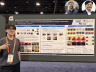
<CVPR 2026 poster session. From left to right: Minseok Seo (KAIST, first author), Mark Hamilton (MIT and Microsoft, second author), and Prof. Changick Kim (KAIST, corresponding author)> From facial recognition on smartphones to humanoid robots, computer vision technology, which serves as the eyes of artificial intelligence (AI), is widely utilized in our daily lives. A joint research team from KAIST and international institutions has developed a technology that allows AI to see the world more clearly with minimal memory, increasing GPU (Graphics Processing Unit) memory efficiency by up to 16 times. This achievement is evaluated as a core technology that will accelerate the era of humanoid robots and on-device AI. <Overview of Upsample Anything. Given a high-resolution image, it is first downsampled to a low-resolution image and then reconstructed through test-time optimization (TTO). During this process, pixel-wise anisotropic kernel parameters are learned. The learned kernels are subsequently applied to low-resolution foundation feature maps to generate high-resolution feature maps. These feature maps are then used to perform pixel-wise anisotropic Joint Bilateral Upsampling, enabling high-quality reconstruction at high resolution> KAIST announced on June 17th that a research team led by Professor Changick Kim from the School of Electrical Engineering, through joint research with researchers from MIT and Microsoft in the United States, has developed 'Upsample Anything,' a universal technology that can enhance the visual performance of AI even with limited GPU memory. Following its acceptance to 'CVPR 2026,' the world's most prestigious conference in the field of artificial intelligence and computer vision, this achievement was awarded the 'CVPR Compute Gold Star' in recognition of its efficient utilization of computational resources. It was also selected as the 'Transparency Champion,' ranking first overall in the category of research process transparency and reproducibility. This is an accomplishment that widely recognizes the core elements of responsible AI research, including research performance, computational resources used, code disclosure, and experimental reproducibility. Recently, humanoid robots, autonomous driving systems, and AI based on world models (AI models that learn and predict the physical environment and changes of the real world) have been compressing input images into low-resolution features (core information extracted from images by AI) to increase computational speed and reduce memory usage. However, during the compression process, a problem occurs where important visual information, such as small objects, thin structures, and minute defects, is lost. Conversely, processing all images at high resolution from the beginning requires massive GPU memory and computational resources, making real-time processing difficult. This has remained an unresolved challenge for a long time in situations where small devices like smartphones or robots, where mobility is crucial, must precisely perceive their surrounding environment. To overcome these limitations, the research team developed a training-free (requiring no additional data training) upsampling technology that restores low-resolution feature information into high resolution by utilizing the edge and structural information of the input image. Existing technologies required a separate retraining or complex optimization process to be applied to new environments or data. In contrast, 'Upsample Anything' developed by the research team can find the optimal restoration method using just a single input image, allowing it to be immediately applied to various environments. In addition, by compressing and utilizing only core information instead of storing and processing all visual information at high resolution, GPU memory usage was significantly reduced. Based on a 224×224 size image (approximately 50,000 pixels) widely used in AI research, the research team restored visual information close to the original with a short calculation of about 0.4 seconds, achieving a performance that improves GPU memory efficiency by up to 16 times. This means that artificial intelligence can perceive its surrounding environment more precisely even with limited computational resources. Therefore, this technology is expected to be widely used in various next-generation artificial intelligence fields, such as small devices like smartphones, as well as humanoid robots that need to accurately identify and manipulate small objects, autonomous driving systems, and on-device AI. <Comparison image illustrating the performance gap with conventional methods (AI-generated). Conventional vision foundation models understand a scene by converting the input image into low-resolution features at a small patch level (left). Upsample Anything restores these low-resolution features to the original resolution level, enabling the AI to comprehend the scene's structure and boundaries with significantly higher precision (right)> Professor Changick Kim said, “This technology is an algorithm that can significantly increase the visual precision of artificial intelligence with fewer resources, and it is expected to accelerate the commercialization of humanoid robots and on-device AI.” He added, “It is even more meaningful because it was recognized at CVPR not only for its performance but also for its computational efficiency and research transparency.” This research was participated in by KAIST PhD student Minseok Seo as the first author, and this achievement was presented on June 7 at 'CVPR 2026,' the world's most prestigious conference in the field of artificial intelligence and computer vision. ※ Paper Title: Upsample Anything: A Simple and Hard to Beat Baseline for Feature Upsampling, DOI:10.48550/arXiv.2511.16301 ※ Author Information: Minseok Seo (KAIST, First Author), Mark Hamilton (MIT, Microsoft, Second Author), Changick Kim (KAIST, Corresponding Author)
-

KAIST Breaks a Major AI Bottleneck with Liquid Coo..
<(From Left) Professor Sung Jin Kim, Professor Ikjin Lee, Dr. Yong Jin Lee, Ph.D candidate Hansol Lee, Ph.D candidate ChulHyun Hwang> AI data centers are often described as “power-hungry giants.” Not only do artificial intelligence computations consume enormous amounts of electricity, but a significant amount of energy is also required to cool the semiconductor chips that heat up during operation. As AI chips continue to deliver higher performance, the amount of heat they generate is increasing rapidly. As a result, conventional air cooling and external copper heat spreaders are approaching their practical limits. To address this challenge, KAIST research team has developed an ultra-high-efficiency liquid-cooling technology that cools semiconductor chips from within. KAIST (President Kwang Hyung Lee) announced on the 16th that a joint research team led by Professor Sung Jin Kim of the Department of Mechanical Engineering and Professor Ikjin Lee of the School of AI and Computing has developed a highly efficient liquid-cooling technology that directly cools high-heat-flux semiconductor chips using room-temperature water. The researchers achieved this by embedding liquid-cooling channels, thinner than a human hair, directly inside a silicon semiconductor chip. The team successfully maintained the chip temperature below 100°C even under extreme heat-generation conditions exceeding 2,000 watts per square centimeter (W/cm²). <Manifold Microchannel Cooling Device Structure for Cooling High-Heat-Generation Semiconductor Chips> The researchers focused on a Manifold MicroChannel (MMC hereafter) structure embedded directly inside a silicon chip. Microchannel cooling removes heat through microscopic fluid channels that are smaller than a human hair. In conventional designs, coolant must travel through numerous microchannels from one end of the chip to the other. This long flow path increases flow resistance and requires greater pumping power to circulate the coolant. The manifold structure developed by the research team distributes coolant through multiple inlet channels and collects it through multiple outlets. An analogy can be drawn to a logistics network: instead of shipping all goods from a single origin to a distant destination, multiple distribution centers are strategically placed to shorten transportation distances. Because the coolant travels only a short distance within each channel, flow resistance is significantly reduced, and the required pumping pressure becomes much lower. Previous MMC designs often suffered from uneven coolant distribution, with some channels receiving too much coolant while others received too little. The research team overcame this challenge by optimizing the structure so that coolant could flow evenly through all microchannels. Through extensive design analysis and advanced simulations, they identified an optimized cooling architecture that delivers high cooling performance while minimizing energy loss. The optimized structure was then fabricated in an actual silicon semiconductor chip and experimentally validated. Under the same temperature-rise condition, the cooling system achieved a coefficient of performance (COP) of 106,000. This is approximately ten times higher than the previous world-leading result of around 10,000 reported in Nature (van Erp et al.) in 2020. In practical terms, it means that only about one-tenth of the pumping power is required to remove the same amount of heat. Notably, this performance was achieved without relying on phase-change cooling, nanoscale surface modifications, or expensive materials such as diamond. Ordinary room-temperature water was used as the coolant. In addition, the device was fabricated using a low-temperature process below 350°C that is compatible with conventional semiconductor manufacturing. This means the technology could be implemented in existing semiconductor foundries without requiring major additional equipment investments. <Fabricated Cooling Device, Experimental Results, and Applications> The technology is expected to help address thermal management challenges in a wide range of high-heat-flux electronic systems, including AI accelerators, high-performance computing (HPC) systems, three-dimensional semiconductor packaging, power electronics, and defense electronics. In particular, data centers are increasingly constrained not only by computing performance but also by cooling power consumption and cooling infrastructure requirements. Technologies that reduce pumping power at the chip level could therefore play an important role in improving the energy efficiency of next-generation data centers and alleviating thermal bottlenecks. <Research Image(AI-generated)> Professor Sung Jin Kim said, “As the performance of AI semiconductors and advanced electronic packaging becomes increasingly limited by heat, we expect this technology to serve as a foundational cooling solution for future high-performance computing systems.” The study was co-first-authored by Young Jin Lee, ChulHyun Hwang, and Hansol Lee from the Department of Mechanical Engineering at KAIST. The research was published on June 15 in the international journal Energy Conversion and Management. Paper title: Highly energy-efficient manifold microchannel for cooling electronics with a coefficient of performance over 100,000 DOI: 10.1016/j.enconman.2026.121422 This research was supported by the Mid-Career Researcher Program of the National Research Foundation of Korea (NRF), funded by the Ministry of Science and ICT (Grant No. 2021R1A2C3011944), and by the Specialized Research Laboratory Program for Ultra-High-Heat-Flux Cooling Systems of the Korea Research Institute for Defense Technology Planning and Advancement (KRIT), funded by the Defense Acquisition Program Administration (Grant No. KRIT-CT-22-022).
-
A Breakthrough Concept in Nano-Printing Technology..
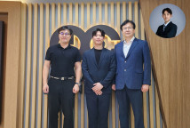
<(From Left) Professor Inkyu Park, Ph.D candidate Byung-Ho Kang, Researcher Jun-Ho Jeong, Professor Junseong Ahn> A breakthrough technology has been developed that allows metal circuits floating on water to be transferred directly onto any desired surface. A South Korean research team has introduced a novel technique capable of transferring ultra-fine nano-circuits onto plant leaves and fruits, as well as curved automotive surfaces and robot exteriors, all without causing any damage. This technology is expected to be widely utilized across various cutting-edge industries, including smart agriculture, wearable healthcare, and bioelectronics. KAIST announced on June 15th that a joint research team led by Distinguished Professor Inkyu Park from the Department of Mechanical Engineering, Dr. Jun-Ho Jeong from the Korea Institute of Machinery and Materials and Professor Junseong Ahn from Korea University has successfully developed "Water-Floating Nano-Transfer Printing (WF-nTP)." This technology enables precision metal thin films floated on water to be transferred onto various 3D surfaces. Conventional nano-transfer printing (nTP), which is widely used to manufacture electronic devices and sensors, typically requires high heat, intense pressure, adhesives, or toxic chemical solvents. Consequently, applying this method to biological tissues or complex curved surfaces that are sensitive to heat and pressure has proven highly challenging. To overcome these limitations, the research team proposed a completely new approach: floating metal circuits on the surface of water. Fabrication: The team deposited an ultra-thin layer of metals such as gold (Au), platinum (Pt), palladium (Pd), or nickel (Ni) onto a polymer mold. Separation: They then used plasma gas which has a high-energy state of ionized gas to selectively remove (etch) a part of the mold. Floating: When this structure is placed in water, water infiltrates through the microscopic gaps, causing the 20-nanometer (nm) thick metal film to float to the surface on its own while perfectly maintaining its original shape. <Overview of the water-floated nano mesh and versatile transfer technique> The research team transferred the metal circuits using a "scooping" method, which involves submerging the target object beneath the floating film and slowly lifting it upward. As the water evaporates, capillary force (the force that moves liquid through narrow spaces) tightly adheres the circuit to the surface. Once the water completely dries, intermolecular forces come into play, securing the circuit firmly in place without the need for any adhesive. Notably, the team also succeeded in transferring circuits onto hydrophobic (water-repellent) surfaces, such as lotus leaves. By adding a small amount of ethanol to the water to lower its surface tension (the property of a liquid surface that causes it to shrink), they effectively overcame a major limitation of conventional technologies. This technology holds immense potential for widespread application because it can adapt to diverse surfaces while flawlessly preserving the nano-patterns. Using this method, the research team fabricated Surface-Enhanced Raman Scattering (SERS) sensors which are used for high-sensitivity detection of trace chemical substances and attached them directly to plant leaves and fruit surfaces. Through this, they successfully detected thiram, a pesticide component, on the surfaces of leaves and fruits. Furthermore, they successfully implemented a wearable, high-performance hydrogen gas sensor by transferring a palladium (Pd) mesh onto highly flexible thermoplastic polyurethane (TPU) fibers. <Research Image(AI-generated)> Distinguished Professor Inkyu Park stated: "This technology is highly significant as it shatters the substrate limitations of conventional nano-transfer printing, allowing nano-patterns to be transferred onto sensitive surfaces like living plant leaves or human skin without heat or adhesives. We expect it to evolve into a core platform technology for wearable sensors and bioelectronics, finding applications in smart agriculture for pesticide detection without damaging crops, wearable health monitoring devices, bioelectronic devices, and electronic skins for next-generation robots." This research, with PhD student Byung-Ho Kang from the KAIST Department of Mechanical Engineering participating as the first author, was published online on March 30, 2026, in the prestigious international academic journal Nature Communications. The study authors include Byung-Ho Kang, Ji-Hwan Ha, Yeongjae Kwon, Sohee Jeon, Donho Lee, Byeongmin Kang, Soon Hyoung Hwang, Junseong Ahn, Jun-Ho Jeong, and Inkyu Park. Meanwhile, this research was conducted with funding from the Ministry of Science and ICT through the National Research Foundation of Korea (NRF) Mid-Career Researcher Support Program, and the Ministry of Trade, Industry and Energy through the Korea Evaluation Institute of Industrial Technology (KEIT) Alchemist Project.
-
How Small Can Semiconductors Get? KAIST Develops A..
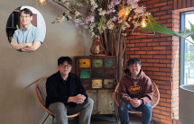
<(From Left) Dr. Tae Hyung Kim, Dr. Juho Lee, (Upper Left) Professor Yong-Hoon Kim> As the global semiconductor industry enters the so-called "2 nm (nanometer, one-billionth of a meter) process" era, the actual size of transistors — the core components of semiconductor chips — still remains above 10 nm. How much smaller, then, can transistors actually get? KAIST researchers have developed a technology to predict that limit through quantum mechanical atom-level calculations. KAIST (President Kwang Hyung Lee) announced on the 14th that a research team led by Professor Yong-Hoon Kim of the School of Electrical Engineering has developed a computational design technology that utilizes computer simulations to analyze and predict the scaling limits of transistors, a key challenge in developing next-generation semiconductor devices. <Research Image(AI-generated)> Transistors are ultra-small switches that turn electrical currents on and off, serving as key components that determine the performance and power efficiency of semiconductor chips that power smartphones, artificial intelligence computers, and more. The semiconductor industry has continuously downsized transistors to achieve higher performance and lower power consumption. However, when the size becomes excessively small, quantum tunneling occurs—a quantum mechanical phenomenon where electrons pass through energy barriers they normally cannot cross—making current control difficult. For this reason, identifying how much smaller transistors can be made within the boundaries of quantum tunneling is a critical task in next-generation semiconductor development. However, it is virtually impossible to experimentally confirm the scaling limits of transistors directly. With current technology, it is difficult to precisely control and quantitatively analyze the contact area where the metal electrode and the semiconductor channel (the pathway through which current flows inside a transistor) meet at the atomic level. The research team resolved this issue by utilizing ab initio or first-principles calculations, a method that computes material properties based solely on fundamental physics laws without relying on experimental data. The research team had previously developed and reported a new theoretical-computational framework called multi-space constrained-search density functional theory (MS-DFT), which extends the scope of first-principles calculations from materials to devices by precisely analyzing the complex quantum phenomena occurring at the interface where metal electrodes and semiconductors meet and across which electrons flow. In this study, the team built on this framework to perform computational transfer length method (TLM) experiments, the gold standard experimental technique for extracting contact resistance (the resistance to current flow occurring at the metal electrode-semiconductor interface). Based on the atomic-level TLM calculations results, they identified the quantum tunneling limit (the length at which electrons stop leaking and begin to allow transistor current control). The research team applied this technology to a monolayer MoS₂ (molybdenum disulfide) device, a representative two-dimensional semiconductor material that can be made as thin as an atomic layer and is a candidate material for next-generation transistor channels. As a result, they were able to quantitatively analyze how deeply electrons penetrate into the channel and how much this hinders current flow control depending on the type of metal electrode and the contact atomic geometry. In other words, they clarified that the limit to how small a transistor can be made varies depending on which metal and contact structure are selected. This implies that the performance and limits of a device can now be predicted in advance solely through computer simulations before the actual transistor fabrication. < Analysis of Contact Resistance and Critical Tunneling Length in Two-Dimensional Semiconductors Using the First-Principles Transfer Length Method > According to the research results, the critical tunneling length—the maximum length at which electrons penetrate into the channel and begin to affect transistor operation—was found not to be a single fixed value. This length emerged as a design variable that changes depending on the work function of the metal (the minimum energy required to remove an electron from a metal) and the contact structure of the interface where the metal and semiconductor meet. This signifies that the extent to which a transistor can be downsized depends on the combination of materials and structural design. In particular, among the candidate metal types and contact structures considered, the research team confirmed that the length where electrons stop leaking could be reduced to less than 4 nm. This result demonstrates the possibility of making transistors even smaller than the levels achieved today. Furthermore, the research team proposed a design strategy for next-generation semiconductor chips that reduce power consumption by combining two-dimensional semiconductors with different properties. This study is significant because it establishes a platform for predicting scaling limits and designing optimal device configurations before actually fabricating semiconductor chips. Through this, it is expected to reduce trial and error and shorten the development period in the process of developing next-generation ultra-small AI semiconductor devices. Professor Yong-Hoon Kim said, "This study is significant because it presents a new physical criterion for defining how small next-generation transistors can become. By computationally analyzing quantum mechanical phenomena in the sub-10 nm regime, which are difficult to probe experimentally, we have opened a path toward utilizing these findings in next-generation transistor design." The study, in which Dr. Tae Hyung Kim participated as the first author, was published online on May 28th in the prestigious computational journal 'npj Computational Materials, a prestigious journal in the field of computational materials science ※ Title of the paper: Ab initio transfer length method simulations of tunneling limits in 2D semiconductors, DOI: https://doi.org/10.1038/s41524-026-02101-1 This research was conducted with support from programs such as the Mid-Career Researcher Program and EDISON 2.0 Program of the National Research Foundation of Korea.

291 Daehak-ro, Yuseong-gu, Daejeon, Korea 34141
KAIST College of Engineering
T.+82-42-350-2114
F.+82-42-350-2210 (2220)
ⓒ KAIST College of Engineering. All rights reserved.