


Students News
-

KAIST & CMU Unveils Amuse, a Songwriting AI-Collab..
Wouldn't it be great if music creators had someone to brainstorm with, help them when they're stuck, and explore different musical directions together? Researchers of KAIST and Carnegie Mellon University (CMU) have developed AI technology similar to a fellow songwriter who helps create music. KAIST (President Kwang-Hyung Lee) has developed an AI-based music creation support system, Amuse, by a research team led by Professor Sung-Ju Lee of the School of Electrical Engineering in collaboration with CMU. The research was presented at the ACM Conference on Human Factors in Computing Systems (CHI), one of the world’s top conferences in human-computer interaction, held in Yokohama, Japan from April 26 to May 1. It received the Best Paper Award, given to only the top 1% of all submissions. < (From left) Professor Chris Donahue of Carnegie Mellon University, Ph.D. Student Yewon Kim and Professor Sung-Ju Lee of the School of Electrical Engineering > The system developed by Professor Sung-Ju Lee’s research team, Amuse, is an AI-based system that converts various forms of inspiration such as text, images, and audio into harmonic structures (chord progressions) to support composition. For example, if a user inputs a phrase, image, or sound clip such as “memories of a warm summer beach”, Amuse automatically generates and suggests chord progressions that match the inspiration. Unlike existing generative AI, Amuse is differentiated in that it respects the user's creative flow and naturally induces creative exploration through an interactive method that allows flexible integration and modification of AI suggestions. The core technology of the Amuse system is a generation method that blends two approaches: a large language model creates music code based on the user's prompt and inspiration, while another AI model, trained on real music data, filters out awkward or unnatural results using rejection sampling. < Figure 1. Amuse system configuration. After extracting music keywords from user input, a large language model-based code progression is generated and refined through rejection sampling (left). Code extraction from audio input is also possible (right). The bottom is an example visualizing the chord structure of the generated code. > The research team conducted a user study targeting actual musicians and evaluated that Amuse has high potential as a creative companion, or a Co-Creative AI, a concept in which people and AI collaborate, rather than having a generative AI simply put together a song. The paper, in which a Ph.D. student Yewon Kim and Professor Sung-Ju Lee of KAIST School of Electrical and Electronic Engineering and Carnegie Mellon University Professor Chris Donahue participated, demonstrated the potential of creative AI system design in both academia and industry. ※ Paper title: Amuse: Human-AI Collaborative Songwriting with Multimodal Inspirations DOI: https://doi.org/10.1145/3706598.3713818 ※ Research demo video: https://youtu.be/udilkRSnftI?si=FNXccC9EjxHOCrm1 ※ Research homepage: https://nmsl.kaist.ac.kr/projects/amuse/ Professor Sung-Ju Lee said, “Recent generative AI technology has raised concerns in that it directly imitates copyrighted content, thereby violating the copyright of the creator, or generating results one-way regardless of the creator’s intention. Accordingly, the research team was aware of this trend, paid attention to what the creator actually needs, and focused on designing an AI system centered on the creator.” He continued, “Amuse is an attempt to explore the possibility of collaboration with AI while maintaining the initiative of the creator, and is expected to be a starting point for suggesting a more creator-friendly direction in the development of music creation tools and generative AI systems in the future.” This research was conducted with the support of the National Research Foundation of Korea with funding from the government (Ministry of Science and ICT). (RS-2024-00337007)
-
KAIST Identifies Master Regulator Blocking Immunot..
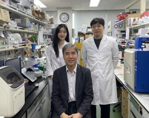
Immune checkpoint inhibitors, a class of immunotherapies that help immune cells attack cancer more effectively, have revolutionized cancer treatment. However, fewer than 20% of patients respond to these treatments, highlighting the urgent need for new strategies tailored to both responders and non-responders. KAIST researchers have discovered that 'DEAD-box helicases 54 (DDX54)', a type of RNA-binding protein, is the master regulator that hinders the effectiveness of immunotherapy—opening a new path for lung cancer treatment. This breakthrough technology has been transferred to faculty startup BioRevert Inc., where it is currently being developed as a companion therapeutic and is expected to enter clinical trials by 2028. < Photo 1. (From left) Researcher Jungeun Lee, Professor Kwang-Hyun Cho and Postdoctoral Researcher Jeong-Ryeol Gong of the Department of Bio and Brain Engineering at KAIST > KAIST (represented by President Kwang-Hyung Lee) announced on April 8 that a research team led by Professor Kwang-Hyun Cho from the Department of Bio and Brain Engineering had identified DDX54 as a critical factor that determines the immune evasion capacity of lung cancer cells. They demonstrated that suppressing DDX54 enhances immune cell infiltration into tumors and significantly improves the efficacy of immunotherapy. Immunotherapy using anti-PD-1 or anti-PD-L1 antibodies is considered a powerful approach in cancer treatment. However, its low response rate limits the number of patients who actually benefit. To identify likely responders, tumor mutational burden (TMB) has recently been approved by the FDA as a key biomarker for immunotherapy. Cancers with high mutation rates are thought to be more responsive to immune checkpoint inhibitors. However, even tumors with high TMB can display an “immune-desert” phenotype—where immune cell infiltration is severely limited—resulting in poor treatment responses. < Figure 1. DDX54 was identified as the master regulator that induces resistance to immunotherapy by orchestrating suppression of immune cell infiltration through cancer tissues as lung cancer cells become immune-evasive > Professor Kwang-Hyun Cho's research team compared transcriptome and genome data of lung cancer patients with immune evasion capabilities through gene regulatory network analysis (A) and discovered DDX54, a master regulator that induces resistance to immunotherapy (B-F). This study is especially significant in that it successfully demonstrated that suppressing DDX54 in immune-desert lung tumors can overcome immunotherapy resistance and improve treatment outcomes. The team used transcriptomic and genomic data from immune-evasive lung cancer patients and employed systems biology techniques to infer gene regulatory networks. Through this analysis, they identified DDX54 as a central regulator in the immune evasion of lung cancer cells. In a syngeneic mouse model, the suppression of DDX54 led to significant increases in the infiltration of anti-cancer immune cells such as T cells and NK cells, and greatly improved the response to immunotherapy. Single-cell transcriptomic and spatial transcriptomic analyses further showed that combination therapy targeting DDX54 promoted the differentiation of T cells and memory T cells that suppress tumors, while reducing the infiltration of regulatory T cells and exhausted T cells that support tumor growth. < Figure 2. In the syngeneic mouse model made of lung cancer cells, it was confirmed that inhibiting DDX54 reversed the immune-evasion ability of cancer cells and enhanced the sensitivity to anti-PD-1 therapy > In a syngeneic mouse model made of lung cancer cells exhibiting immunotherapy resistance, the treatment applied after DDX54 inhibition resulted in statistically significant inhibition of lung cancer growth (B-D) and a significant increase in immune cell infiltration into the tumor tissue (E, F). The mechanism is believed to involve DDX54 suppression inactivating signaling pathways such as JAK-STAT, MYC, and NF-κB, thereby downregulating immune-evasive proteins CD38 and CD47. This also reduced the infiltration of circulating monocytes—which promote tumor development—and promoted the differentiation of M1 macrophages that play anti-tumor roles. Professor Kwang-Hyun Cho stated, “We have, for the first time, identified a master regulatory factor that enables immune evasion in lung cancer cells. By targeting this factor, we developed a new therapeutic strategy that can induce responsiveness to immunotherapy in previously resistant cancers.” He added, “The discovery of DDX54—hidden within the complex molecular networks of cancer cells—was made possible through the systematic integration of systems biology, combining IT and BT.” The study, led by Professor Kwang-Hyun Cho, was published in the Proceedings of the National Academy of Sciences of the United States of America (PNAS) on April 2, 2025, with Jeong-Ryeol Gong being the first author, Jungeun Lee, a co-first author, and Younghyun Han, a co-author of the article. < Figure 3. Single-cell transcriptome and spatial transcriptome analysis confirmed that knockdown of DDX54 increased immune cell infiltration into cancer tissues > In a syngeneic mouse model made of lung cancer cells that underwent immunotherapy in combination with DDX54 inhibition, single-cell transcriptome (H-L) and spatial transcriptome (A-G) analysis of immune cells infiltrating inside cancer tissues were performed. As a result, it was confirmed that anticancer immune cells such as T cells, B cells, and NK cells actively infiltrated the core of lung cancer tissues when DDX54 inhibition and immunotherapy were concurrently administered. (Paper title: “DDX54 downregulation enhances anti-PD1 therapy in immune-desert lung tumors with high tumor mutational burden,” DOI: https://doi.org/10.1073/pnas.2412310122) This work was supported by the Ministry of Science and ICT and the National Research Foundation of Korea through the Mid-Career Research Program and Basic Research Laboratory Program. < Figure 4. The identified master regulator DDX54 was confirmed to induce CD38 and CD47 expression through Jak-Stat3, MYC, and NF-κB activation. > DDX54 activates the Jak-Stat3, MYC, and NF-κB pathways in lung cancer cells to increase CD38 and CD47 expression (A-G). This creates a cancer microenvironment that contributes to cancer development (H) and ultimately induces immune anticancer treatment resistance. < Figure 5. It was confirmed that an immune-inflamed environment can be created by combining DDX54 inhibition and immune checkpoint inhibitor (ICI) therapy. > When DDX54 inhibition and ICI therapy are simultaneously administered, the cancer cell characteristics change, the immune evasion ability is restored, and the environment is transformed into an ‘immune-activated’ environment in which immune cells easily infiltrate cancer tissues. This strengthens the anticancer immune response, thereby increasing the sensitivity of immunotherapy even in lung cancer tissues that previously had low responsiveness to immunotherapy.
-
KAIST Develops Eco-Friendly, Nylon-Like Plastic Us..
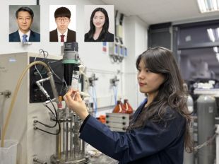
Poly(ester amide) amide is a next-generation material that combines the advantages of PET (polyester) and nylon (polyamide), two widely used plastics. However, it could only be produced from fossil fuels, which posed environmental concerns. Using microorganisms, KAIST researchers have successfully developed a new bio-based plastic to replace conventional plastic. < Photo 1. (From left) Professor Sang Yup Lee, Dr. Tong Un Chae, Dr. So Young Choi, and Ph.D. candidate Da-Hee Ahn of the Department of Chemical and Biomolecular Engineering > KAIST (represented by President Kwang Hyung Lee) announced on the 20th of March that a research team led by Distinguished Professor Sang Yup Lee from the Department of Chemical and Biomolecular Engineering has developed microbial strains through systems metabolic engineering to produce various eco-friendly, bio-based poly(ester amide)s. The team collaborated with researchers from the Korea Research Institute of Chemical Technology (KRICT, President Young-Kook Lee) to analyze and confirm the properties of the resulting plastic. Professor Sang Yup Lee’s research team designed new metabolic pathways that do not naturally exist in microorganisms, and developed a platform microbial strain capable of producing nine different types of poly(ester amide)s, including poly(3-hydroxybutyrate-ran-3-aminopropionate) and poly(3-hydroxybutyrate-ran-4-aminobutyrate). Using glucose derived from abundant biomass sources such as waste wood and weeds, the team successfully produced poly(ester amide)s in an eco-friendly manner. The researchers also confirmed the potential for industrial-scale production by demonstrating high production efficiency (54.57 g/L) using fed-batch fermentation of the engineered strain. In collaboration with researchers Haemin Jeong and Jihoon Shin from KRICT, the KAIST team analyzed the properties of the bio-based plastic and found that it exhibited characteristics similar to high-density polyethylene (HDPE). This means the new plastic is not only eco-friendly but also strong and durable enough to replace conventional plastics. < Figure 1. New-to-nature metabolic pathways for the production of poly(ester amide)s (PEAs). > The engineered strains and strategies developed in this study are expected to be useful not only for producing various poly(ester amide)s but also for constructing metabolic pathways for the biosynthesis of other types of polymers. Professor Sang Yup Lee stated, “This study is the first to demonstrate the possibility of producing poly(ester amide)s (plastics) through a renewable bio-based chemical process rather than relying on the petroleum-based chemical industry. We plan to further enhance the production yield and efficiency through continued research.” The study was published online on March 17 in the international journal Nature Chemical Biology. ·Title: Biosynthesis of poly(ester amide)s in engineered Escherichia coli ·DOI: 10.1038/s41589-025-01842-2 ·Authors: A total of seven authors including Tong Un Chae (KAIST, first author), So Young Choi (KAIST, second author), Da-Hee Ahn (KAIST, third author), Woo Dae Jang (KAIST, fourth author), Haemin Jeong (KRICT, fifth author), Jihoon Shin (KRICT, sixth author), and Sang Yup Lee (KAIST, corresponding author). This research was supported by the Ministry of Science and ICT (MSIT) under the Eco-Friendly Chemical Technology Development Project as part of the "Next-Generation Biorefinery Technology Development to Lead the Bio-Chemical Industry" initiative (project led by Distinguished Professor Sang Yup Lee at KAIST).
-
KAIST Develops World-Leading Ammonia Catalyst for ..
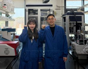
Hydrogen production using renewable energy is a key technology for eco-friendly energy and chemical production. However, storing and transporting hydrogen remains a challenge. To address this, researchers worldwide are investigating methods to store hydrogen in the form of ammonia (NH₃), which is carbon-free and easier to liquify. A research team at KAIST has successfully developed a high-performance catalyst that enables ammonia synthesis at very low temperatures and pressures without energy loss. KAIST (represented by President Kwang Hyung Lee) announced on the 11th of March that a research team led by Professor Minkee Choi from the Department of Chemical and Biomolecular Engineering has developed an innovative catalytic system that significantly enhances ammonia production while drastically reducing energy consumption and CO₂ emissions. < (From left) Baek Ye-jun, Ph.D. candidate in the Department of Biochemical Engineering, Professor Choi Min-ki > Currently, ammonia is produced using the Haber-Bosch process, a technology over a century old that relies on iron (Fe)-based catalysts. This method requires extreme conditions—temperatures above 500°C and pressures exceeding 100 atmospheres—resulting in enormous energy consumption and contributing significantly to global CO₂ emissions. Additionally, ammonia is primarily produced in large-scale industrial plants, leading to high distribution costs. As an alternative, there is growing interest in an eco-friendly process that synthesizes ammonia using green hydrogen—produced via water electrolysis—under mild conditions (300°C, 10 atmospheres). However, developing catalysts that can achieve high ammonia productivity at such low temperatures and pressures is essential, as current technologies struggle to maintain efficiency under these conditions. The research team developed a novel catalyst by incorporating ruthenium (Ru) nanoparticles and highly basic barium oxide (BaO) particles onto a conductive carbon surface, allowing it to function like a chemical capacitor*. *Capacitor: A device that stores electrical energy by separating positive and negative charges. During ammonia synthesis, hydrogen molecules (H₂) first dissociate into hydrogen atoms (H) on the ruthenium catalyst. These hydrogen atoms are further split into protons (H⁺) and electrons (e⁻). The study revealed that the acidic protons are stored in the strongly basic BaO, while the remaining electrons are separated and stored in ruthenium and carbon. This unique chemical capacitor effect significantly enhances the ruthenium catalyst's electron density, accelerating nitrogen (N₂) dissociation—the rate-limiting step of ammonia synthesis—thereby dramatically increasing catalytic activity. Furthermore, the team discovered that optimizing the nanostructure of the carbon material further boosts the electron density of ruthenium, maximizing catalytic performance. As a result, the new catalyst demonstrated over seven times higher ammonia synthesis performance compared to state-of-the-art catalysts under mild conditions (300°C, 10 atm). < Schematic diagram showing the mechanism of ruthenium catalyst activity enhancement by barium oxide cocatalyst > Professor Minkee Choi stated, “This research has garnered significant attention for demonstrating that catalytic activity can be greatly enhanced by controlling electron transfer within a thermal catalytic reaction system, not just in electrochemical processes.” He further explained, “Our findings confirm that high-performance catalysts can enable efficient ammonia synthesis under low-temperature and low-pressure conditions. This could shift ammonia production from centralized, large-scale industrial plants to decentralized, small-scale production, making the hydrogen economy more sustainable and flexible.” The study was led by Professor Minkee Choi as corresponding author and Yaejun Baik, a Ph.D. candidate, as first author. The research findings were published in Nature Catalysis on February 24. (Paper title: “Electron and proton storage on separate Ru and BaO domains mediated by conductive low-work-function carbon to accelerate ammonia synthesis,” https://doi.org/10.1038/s41929-025-01302-z) This research was supported by the Korea Institute of Energy Research and the National Research Foundation of Korea.
-
No More Touch Issues on Rainy Days! KAIST Develops..
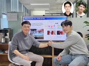
< Photo 1. (From left) Professor Jun-Bo Yoon and Dr. Jae-Soon Yang of KAIST with (top left) Myung-Kun Chung, a student of integrated master > Recent advancements in robotics have enabled machines to handle delicate objects like eggs with precision, thanks to highly integrated pressure sensors that provide detailed tactile feedback. However, even the most advanced robots struggle to accurately detect pressure in complex environments involving water, bending, or electromagnetic interference. A research team at KAIST has successfully developed a pressure sensor that operates stably without external interference, even on wet surfaces like a smartphone screen covered in water, achieving human-level tactile sensitivity. KAIST (represented by President Kwang Hyung Lee) announced on the 10th of March that a research team led by Professor Jun-Bo Yoon from the School of Electrical Engineering has developed a high-resolution pressure sensor that remains unaffected by external interference such as "ghost touches" caused by moisture on touchscreens. Capacitive pressure sensors, widely used in touch systems due to their simple structure and durability, are essential components of human-machine interface (HMI) technologies in smartphones, wearable devices, and robots. However, they are prone to malfunctions caused by water droplets, electromagnetic interference, and curves. < Figure 1. (Left) Schematic diagram of a smartphone surface that does not respond well to touch when wet on a rainy day. (Center) Schematic diagram of an unintended sensor malfunction in a situation where interference exists. (Right) Simulation results of electric field distribution in normal situations and situations where interference exists. When interference exists, distortion of the fringe field occurs. > To address these issues, the research team investigated the root causes of interference in capacitive pressure sensors. They identified that the "fringe field" generated at the sensor’s edges is particularly susceptible to external disturbances. The researchers concluded that, to fundamentally resolve this issue, suppressing the fringe field was necessary. Through theoretical analysis, they determined that reducing the electrode spacing to the nanometer scale could effectively minimize the fringe field to below a few percent. < Figure 2. (Left) Photograph of the nano-gap pressure sensor developed in this study. (Center) Schematic diagram showing that the fringe field is suppressed due to the nano-gap design, effectively blocking external interference. (Right) Electron microscope image of the actually manufactured nano-gap pressure sensor. > Utilizing proprietary micro/nanofabrication techniques, the team developed a nanogap pressure sensor with an electrode spacing of 900 nanometers (nm). This newly developed sensor reliably detected pressure regardless of the material exerting force and remained unaffected by bending or electromagnetic interference. Furthermore, the team successfully implemented an artificial tactile system utilizing the developed sensor’s characteristics. Human skin contains specialized pressure receptors called Merkel’s disks. To artificially mimic them, the exclusive detection of pressure was necessary, but hadn’t been achieved by conventional sensors. Professor Yoon’s research team overcame these challenges, developing a sensor achieving a density comparable to Merkel’s discs and enabling wireless, high-precision pressure sensing. < Figure 3. (Left) Schematic diagram of a nano-gap pressure sensor that is free from interference and has high resolution to simulate the pressure detection method of the human body. (Right) A wireless artificial tactile system implemented using a nano-gap pressure sensor to pick up a wet object. It does not react even when water gets on the surface and only precisely detects pressure. > To explore potential applications, the researcher also developed a force touch pad system, demonstrating its ability to capture pressure magnitude and distribution with high resolution and without interference. Professor Yoon stated, “Our nanogap pressure sensor operates reliably even in rainy conditions or sweaty environments, eliminating common touch malfunctions. We believe this innovation will significantly enhance everyday user experiences.” He added, “This technology has the potential to revolutionize various fields, including precision tactile sensors for robotics, medical wearable devices, and next-generation augmented reality (AR) and virtual reality (VR) interfaces.” < Figure 4. (Left) Schematic diagram of the force touch pad system implemented using a nano gap pressure sensor and the situation where water is on the sensor. (Middle) Multi-touch measurement results using the force touch pad system in the situation where water is on the sensor. (Right) 3D measurement results that precisely show the size and distribution of pressure without interference or cross-interference by water on the sensor. > The study was led by Jae-Soon Yang (Ph.D.), Myung-Kun Chung (Ph.D. candidate), and Jae-Young Yoo (Assistant Professor at Sungkyunkwan University, a KAIST Ph.D. graduate). The research findings were published in Nature Communications on February 27, 2025. (Paper title: “Interference-Free Nanogap Pressure Sensor Array with High Spatial Resolution for Wireless Human-Machine Interface Applications”, DOI: 10.1038/s41467-025-57232-8) This study was supported by the National Research Foundation of Korea’s Mid-Career Researcher Program and Leading Research Center Support Program.
-
KAIST Develops Wearable Carbon Dioxide Sensor to E..
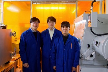
- Professor Seunghyup Yoo’s research team of the School of Electrical Engineering developed an ultralow-power carbon dioxide (CO2) sensor using a flexible and thin organic photodiode, and succeeded in real-time breathing monitoring by attaching it to a commercial mask - Wearable devices with features such as low power, high stability, and flexibility can be utilized for early diagnosis of various diseases such as chronic obstructive pulmonary disease and sleep apnea < Photo 1. From the left, School of Electrical Engineering, Ph.D. candidate DongHo Choi, Professor Seunghyup Yoo, and Department of Materials Science and Engineering, Bachelor’s candidate MinJae Kim > Carbon dioxide (CO2) is a major respiratory metabolite, and continuous monitoring of CO2 concentration in exhaled breath is not only an important indicator for early detection and diagnosis of respiratory and circulatory system diseases, but can also be widely used for monitoring personal exercise status. KAIST researchers succeeded in accurately measuring CO2 concentration by attaching it to the inside of a mask. KAIST (President Kwang-Hyung Lee) announced on the 10th that Professor Seunghyup Yoo's research team in the Department of Electrical and Electronic Engineering developed a low-power, high-speed wearable CO2 sensor capable of stable breathing monitoring in real time. Existing non-invasive CO2 sensors had limitations in that they were large in size and consumed high power. In particular, optochemical CO2 sensors using fluorescent molecules have the advantage of being miniaturized and lightweight, but due to the photodegradation phenomenon of dye molecules, they are difficult to use stably for a long time, which limits their use as wearable healthcare sensors. Optochemical CO2 sensors utilize the fact that the intensity of fluorescence emitted from fluorescent molecules decreases depending on the concentration of CO2, and it is important to effectively detect changes in fluorescence light. To this end, the research team developed a low-power CO2 sensor consisting of an LED and an organic photodiode surrounding it. Based on high light collection efficiency, the sensor, which minimizes the amount of excitation light irradiated on fluorescent molecules, achieved a device power consumption of 171 μW, which is tens of times lower than existing sensors that consume several mW. < Figure 1. Structure and operating principle of the developed optochemical carbon dioxide (CO2) sensor. Light emitted from the LED is converted into fluorescence through the fluorescent film, reflected from the light scattering layer, and incident on the organic photodiode. CO2 reacts with a small amount of water inside the fluorescent film to form carbonic acid (H2CO3), which increases the concentration of hydrogen ions (H+), and the fluorescence intensity due to 470 nm excitation light decreases. The circular organic photodiode with high light collection efficiency effectively detects changes in fluorescence intensity, lowers the power required light up the LED, and reduces light-induced deterioration. > The research team also elucidated the photodegradation path of fluorescent molecules used in CO2 sensors, revealed the cause of the increase in error over time in photochemical sensors, and suggested an optical design method to suppress the occurrence of errors. Based on this, the research team developed a sensor that effectively reduces errors caused by photodegradation, which was a chronic problem of existing photochemical sensors, and can be used continuously for up to 9 hours while existing technologies based on the same material can be used for less than 20 minutes, and can be used multiple times when replacing the CO2 detection fluorescent film. < Figure 2. Wearable smart mask and real-time breathing monitoring. The fabricated sensor module consists of four elements (①: gas-permeable light-scattering layer, ②: color filter and organic photodiode, ③: light-emitting diode, ④: CO2-detecting fluorescent film). The thin and light sensor (D1: 400 nm, D2: 470 nm) is attached to the inside of the mask to monitor the wearer's breathing in real time. > The developed sensor accurately measured CO2 concentration by being attached to the inside of a mask based on the advantages of being light (0.12 g), thin (0.7 mm), and flexible. In addition, it showed fast speed and high resolution that can monitor respiratory rate by distinguishing between inhalation and exhalation in real time. < Photo 2. The developed sensor attached to the inside of the mask > Professor Seunghyup Yoo said, "The developed sensor has excellent characteristics such as low power, high stability, and flexibility, so it can be widely applied to wearable devices, and can be used for the early diagnosis of various diseases such as hypercapnia, chronic obstructive pulmonary disease, and sleep apnea." He added, "In particular, it is expected to be used to improve side effects caused by rebreathing in environments where dust is generated or where masks are worn for long periods of time, such as during seasonal changes." This study, in which KAIST's Department of Materials Science and Engineering's undergraduate student Minjae Kim and School of Electrical Engineering's doctoral student Dongho Choi participated as joint first authors, was published in the online version of Cell's sister journal, Device, on the 22nd of last month. (Paper title: Ultralow-power carbon dioxide sensor for real-time breath monitoring) DOI: https://doi.org/10.1016/j.device.2024.100681 < Photo 3. From the left, Professor Seunghyup Yoo of the School of Electrical Engineering, MinJae Kim, an undergraduate student in the Department of Materials Science and Engineering, and Dongho Choi, a doctoral student in the School of Electrical Engineering > This study was supported by the Ministry of Trade, Industry and Energy's Materials and Components Technology Development Project, the National Research Foundation of Korea's Original Technology Development Project, and the KAIST Undergraduate Research Participation Project. This work was supported by the (URP) program.
-
KAIST Discovers Molecular Switch that Reverses Can..
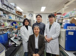
< (From left) PhD student Seoyoon D. Jeong, (bottom) Professor Kwang-Hyun Cho, (top) Dr. Dongkwan Shin, Dr. Jeong-Ryeol Gong > Professor Kwang-Hyun Cho’s research team has recently been highlighted for their work on developing an original technology for cancer reversal treatment that does not kill cancer cells but only changes their characteristics to reverse them to a state similar to normal cells. This time, they have succeeded in revealing for the first time that a molecular switch that can induce cancer reversal at the moment when normal cells change into cancer cells is hidden in the genetic network. KAIST (President Kwang-Hyung Lee) announced on the 5th of February that Professor Kwang-Hyun Cho's research team of the Department of Bio and Brain Engineering has succeeded in developing a fundamental technology to capture the critical transition phenomenon at the moment when normal cells change into cancer cells and analyze it to discover a molecular switch that can revert cancer cells back into normal cells. A critical transition is a phenomenon in which a sudden change in state occurs at a specific point in time, like water changing into steam at 100℃. This critical transition phenomenon also occurs in the process in which normal cells change into cancer cells at a specific point in time due to the accumulation of genetic and epigenetic changes. The research team discovered that normal cells can enter an unstable critical transition state where normal cells and cancer cells coexist just before they change into cancer cells during tumorigenesis, the production or development of tumors, and analyzed this critical transition state using a systems biology method to develop a cancer reversal molecular switch identification technology that can reverse the cancerization process. They then applied this to colon cancer cells and confirmed through molecular cell experiments that cancer cells can recover the characteristics of normal cells. This is an original technology that automatically infers a computer model of the genetic network that controls the critical transition of cancer development from single-cell RNA sequencing data, and systematically finds molecular switches for cancer reversion by simulation analysis. It is expected that this technology will be applied to the development of reversion therapies for other cancers in the future. Professor Kwang-Hyun Cho said, "We have discovered a molecular switch that can revert the fate of cancer cells back to a normal state by capturing the moment of critical transition right before normal cells are changed into an irreversible cancerous state." < Figure 1. Overall conceptual framework of the technology that automatically constructs a molecular regulatory network from single-cell RNA sequencing data of colon cancer cells to discover molecular switches for cancer reversion through computer simulation analysis. Professor Kwang-Hyun Cho's research team established a fundamental technology for automatic construction of a computer model of a core gene network by analyzing the entire process of tumorigenesis of colon cells turning into cancer cells, and developed an original technology for discovering the molecular switches that can induce cancer cell reversal through attractor landscape analysis. > He continued, "In particular, this study has revealed in detail, at the genetic network level, what changes occur within cells behind the process of cancer development, which has been considered a mystery until now." He emphasized, "This is the first study to reveal that an important clue that can revert the fate of tumorigenesis is hidden at this very critical moment of change." < Figure 2. Identification of tumor transition state using single-cell RNA sequencing data from colorectal cancer. Using single-cell RNA sequencing data from colorectal cancer patient-derived organoids for normal and cancerous tissues, a critical transition was identified in which normal and cancerous cells coexist and instability increases (a-d). The critical transition was confirmed to show intermediate levels of major phenotypic features related to cancer or normal tissues that are indicative of the states between the normal and cancerous cells (e). > The results of this study, conducted by KAIST Dr. Dongkwan Shin (currently at the National Cancer Center), Dr. Jeong-Ryeol Gong, and doctoral student Seoyoon D. Jeong jointly with a research team at Seoul National University that provided the organoids (in vitro cultured tissues) from colon cancer patient, were published as an online paper in the international journal ‘Advanced Science’ published by Wiley on January 22nd. (Paper title: Attractor landscape analysis reveals a reversion switch in the transition of colorectal tumorigenesis) (DOI: https://doi.org/10.1002/advs.202412503) < Figure 3. Reconstruction of a dynamic network model for the transition state of colorectal cancer. A new technology was established to build a gene network computer model that can simulate the dynamic changes between genes by integrating single-cell RNA sequencing data and existing experimental results on gene-to-gene interactions in the critical transition of cancer. (a). Using this technology, a gene network computer model for the critical transition of colorectal cancer was constructed, and the distribution of attractors representing normal and cancer cell phenotypes was investigated through attractor landscape analysis (b-e). > This study was conducted with the support of the National Research Foundation of Korea under the Ministry of Science and ICT through the Mid-Career Researcher Program and Basic Research Laboratory Program and the Disease-Centered Translational Research Project of the Korea Health Industry Development Institute (KHIDI) of the Ministry of Health and Welfare. < Figure 4. Quantification of attractor landscapes and discovery of transcription factors for cancer reversibility through perturbation simulation analysis. A methodology for implementing discontinuous attractor landscapes continuously from a computer model of gene networks and quantifying them as cancer scores was introduced (a), and attractor landscapes for the critical transition of colorectal cancer were secured (b-d). By tracking the change patterns of normal and cancer cell attractors through perturbation simulation analysis for each gene, the optimal combination of transcription factors for cancer reversion was discovered (e-h). This was confirmed in various parameter combinations as well (i). > < Figure 5. Identification and experimental validation of the optimal target gene for cancer reversion. Among the common target genes of the discovered transcription factor combinations, we identified cancer reversing molecular switches that are predicted to suppress cancer cell proliferation and restore the characteristics of normal colon cells (a-d). When inhibitors for the molecular switches were treated to organoids derived from colon cancer patients, it was confirmed that cancer cell proliferation was suppressed and the expression of key genes related to cancer development was inhibited (e-h), and a group of genes related to normal colon epithelium was activated and transformed into a state similar to normal colon cells (i-j). > < Figure 6. Schematic diagram of the research results. Professor Kwang-Hyun Cho's research team developed an original technology to systematically discover key molecular switches that can induce reversion of colon cancer cells through a systems biology approach using an attractor landscape analysis of a genetic network model for the critical transition at the moment of transformation from normal cells to cancer cells, and verified the reversing effect of actual colon cancer through cellular experiments. >
-
KAIST Develops AI-Driven Performance Prediction Mo..
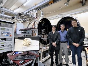
< (From left) PhD candidate Youngho Kim, Professor Wonho Choe, and PhD candidate Jaehong Park from the Department of Nuclear and Quantum Engineering > Hall thrusters, a key space technology for missions like SpaceX's Starlink constellation and NASA's Psyche asteroid mission, are high-efficiency electric propulsion devices using plasma technology*. The KAIST research team announced that the AI-designed Hall thruster developed for CubeSats will be installed on the KAIST-Hall Effect Rocket Orbiter (K-HERO) CubeSat to demonstrate its in-orbit performance during the fourth launch of the Korean Launch Vehicle called Nuri rocket (KSLV-2) scheduled for November this year. *Plasma is one of the four states of matter, where gases are heated to high energies, causing them to separate into charged ions and electrons. Plasma is used not only in space electric propulsion but also in semiconductor manufacturing, display processes, and sterilization devices. On February 3rd, the research team from the KAIST Department of Nuclear and Quantum Engineering’s Electric Propulsion Laboratory, led by Professor Wonho Choe, announced the development of an AI-based technique to accurately predict the performance of Hall thrusters, the engines of satellites and space probes. Hall thrusters provide high fuel efficiency, requiring minimal propellant to achieve significant acceleration of spacecrafts or satellites while producing substantial thrust relative to power consumption. Due to these advantages, Hall thrusters are widely used in various space missions, including the formation flight of satellite constellations, deorbiting maneuvers for space debris mitigation, and deep space missions such as asteroid exploration. As the space industry continues to grow during the NewSpace era, the demand for Hall thrusters suited to diverse missions is increasing. To rapidly develop highly efficient, mission-optimized Hall thrusters, it is essential to predict thruster performance accurately from the design phase. However, conventional methods have limitations, as they struggle to handle the complex plasma phenomena within Hall thrusters or are only applicable under specific conditions, leading to lower prediction accuracy. The research team developed an AI-based performance prediction technique with high accuracy, significantly reducing the time and cost associated with the iterative design, fabrication, and testing of thrusters. Since 2003, Professor Wonho Choe’s team has been leading research on electric propulsion development in Korea. The team applied a neural network ensemble model to predict thruster performance using 18,000 Hall thruster training data points generated from their in-house numerical simulation tool. The in-house numerical simulation tool, developed to model plasma physics and thrust performance, played a crucial role in providing high-quality training data. The simulation’s accuracy was validated through comparisons with experimental data from ten KAIST in-house Hall thrusters, with an average prediction error of less than 10%. < Figure 1. This research has been selected as the cover article for the March 2025 issue (Volume 7, Issue 3) of the AI interdisciplinary journal, Advanced Intelligent Systems. > The trained neural network ensemble model acts as a digital twin, accurately predicting the Hall thruster performance within seconds based on thruster design variables. Notably, it offers detailed analyses of performance parameters such as thrust and discharge current, accounting for Hall thruster design variables like propellant flow rate and magnetic field—factors that are challenging to evaluate using traditional scaling laws. This AI model demonstrated an average prediction error of less than 5% for the in-house 700 W and 1 kW KAIST Hall thrusters and less than 9% for a 5 kW high-power Hall thruster developed by the University of Michigan and the U.S. Air Force Research Laboratory. This confirms the broad applicability of the AI prediction method across different power levels of Hall thrusters. Professor Wonho Choe stated, “The AI-based prediction technique developed by our team is highly accurate and is already being utilized in the analysis of thrust performance and the development of highly efficient, low-power Hall thrusters for satellites and spacecraft. This AI approach can also be applied beyond Hall thrusters to various industries, including semiconductor manufacturing, surface processing, and coating, through ion beam sources.” < Figure 2. The AI-based prediction technique developed by the research team accurately predicts thrust performance based on design variables, making it highly valuable for the development of high-efficiency Hall thrusters. The neural network ensemble processes design variables, such as channel geometry and magnetic field information, and outputs key performance metrics like thrust and prediction accuracy, enabling efficient thruster design and performance analysis. > Additionally, Professor Choe mentioned, “The CubeSat Hall thruster, developed using the AI technique in collaboration with our lab startup—Cosmo Bee, an electric propulsion company—will be tested in orbit this November aboard the K-HERO 3U (30 x 10 x 10 cm) CubeSat, scheduled for launch on the fourth flight of the KSLV-2 Nuri rocket.” This research was published online in Advanced Intelligent Systems on December 25, 2024 with PhD candidate Jaehong Park as the first author and was selected as the journal’s cover article, highlighting its innovation. < Figure 3. Image of the 150 W low-power Hall thruster for small and micro satellites, developed in collaboration with Cosmo Bee and the KAIST team. The thruster will be tested in orbit on the K-HERO CubeSat during the KSLV-2 Nuri rocket’s fourth launch in Q4 2025. > This research was supported by the National Research Foundation of Korea’s Space Pioneer Program (200mN High Thrust Electric Propulsion System Development). (Paper Title: Predicting Performance of Hall Effect Ion Source Using Machine Learning, DOI: https://doi.org/10.1002/aisy.202400555 ) < Figure 4. Graphs of the predicted thrust and discharge current of KAIST’s 700 W Hall thruster using the AI model (HallNN). The left image shows the Hall thruster operating in KAIST Electric Propulsion Laboratory’s vacuum chamber, while the center and right graphs present the prediction results for thrust and discharge current based on anode mass flow rate. The red lines represent AI predictions, and the blue dots represent experimental results, with a prediction error of less than 5%. >
-
KAIST Develops Neuromorphic Semiconductor Chip tha..
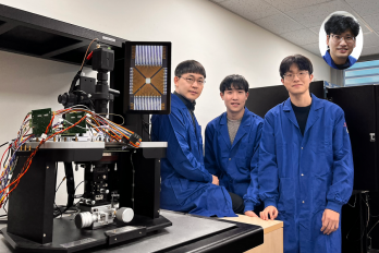
< Photo. The research team of the School of Electrical Engineering posed by the newly deveoped processor. (From center to the right) Professor Young-Gyu Yoon, Integrated Master's and Doctoral Program Students Seungjae Han and Hakcheon Jeong and Professor Shinhyun Choi > - Professor Shinhyun Choi and Professor Young-Gyu Yoon’s Joint Research Team from the School of Electrical Engineering developed a computing chip that can learn, correct errors, and process AI tasks - Equipping a computing chip with high-reliability memristor devices with self-error correction functions for real-time learning and image processing Existing computer systems have separate data processing and storage devices, making them inefficient for processing complex data like AI. A KAIST research team has developed a memristor-based integrated system similar to the way our brain processes information. It is now ready for application in various devices including smart security cameras, allowing them to recognize suspicious activity immediately without having to rely on remote cloud servers, and medical devices with which it can help analyze health data in real time. KAIST (President Kwang Hyung Lee) announced on the 17th of January that the joint research team of Professor Shinhyun Choi and Professor Young-Gyu Yoon of the School of Electrical Engineering has developed a next-generation neuromorphic semiconductor-based ultra-small computing chip that can learn and correct errors on its own. < Figure 1. Scanning electron microscope (SEM) image of a computing chip equipped with a highly reliable selector-less 32×32 memristor crossbar array (left). Hardware system developed for real-time artificial intelligence implementation (right). > What is special about this computing chip is that it can learn and correct errors that occur due to non-ideal characteristics that were difficult to solve in existing neuromorphic devices. For example, when processing a video stream, the chip learns to automatically separate a moving object from the background, and it becomes better at this task over time. This self-learning ability has been proven by achieving accuracy comparable to ideal computer simulations in real-time image processing. The research team's main achievement is that it has completed a system that is both reliable and practical, beyond the development of brain-like components. The research team has developed the world's first memristor-based integrated system that can adapt to immediate environmental changes, and has presented an innovative solution that overcomes the limitations of existing technology. < Figure 2. Background and foreground separation results of an image containing non-ideal characteristics of memristor devices (left). Real-time image separation results through on-device learning using the memristor computing chip developed by our research team (right). > At the heart of this innovation is a next-generation semiconductor device called a memristor*. The variable resistance characteristics of this device can replace the role of synapses in neural networks, and by utilizing it, data storage and computation can be performed simultaneously, just like our brain cells. *Memristor: A compound word of memory and resistor, next-generation electrical device whose resistance value is determined by the amount and direction of charge that has flowed between the two terminals in the past. The research team designed a highly reliable memristor that can precisely control resistance changes and developed an efficient system that excludes complex compensation processes through self-learning. This study is significant in that it experimentally verified the commercialization possibility of a next-generation neuromorphic semiconductor-based integrated system that supports real-time learning and inference. This technology will revolutionize the way artificial intelligence is used in everyday devices, allowing AI tasks to be processed locally without relying on remote cloud servers, making them faster, more privacy-protected, and more energy-efficient. “This system is like a smart workspace where everything is within arm’s reach instead of having to go back and forth between desks and file cabinets,” explained KAIST researchers Hakcheon Jeong and Seungjae Han, who led the development of this technology. “This is similar to the way our brain processes information, where everything is processed efficiently at once at one spot.” The research was conducted with Hakcheon Jeong and Seungjae Han, the students of Integrated Master's and Doctoral Program at KAIST School of Electrical Engineering being the co-first authors, the results of which was published online in the international academic journal, Nature Electronics, on January 8, 2025. *Paper title: Self-supervised video processing with self-calibration on an analogue computing platform based on a selector-less memristor array ( https://doi.org/10.1038/s41928-024-01318-6 ) This research was supported by the Next-Generation Intelligent Semiconductor Technology Development Project, Excellent New Researcher Project and PIM AI Semiconductor Core Technology Development Project of the National Research Foundation of Korea, and the Electronics and Telecommunications Research Institute Research and Development Support Project of the Institute of Information & communications Technology Planning & Evaluation.
-
KAIST Develops Insect-Eye-Inspired Camera Capturin..
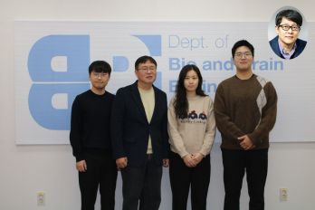
< (From left) Bio and Brain Engineering PhD Student Jae-Myeong Kwon, Professor Ki-Hun Jeong, PhD Student Hyun-Kyung Kim, PhD Student Young-Gil Cha, and Professor Min H. Kim of the School of Computing > The compound eyes of insects can detect fast-moving objects in parallel and, in low-light conditions, enhance sensitivity by integrating signals over time to determine motion. Inspired by these biological mechanisms, KAIST researchers have successfully developed a low-cost, high-speed camera that overcomes the limitations of frame rate and sensitivity faced by conventional high-speed cameras. KAIST (represented by President Kwang Hyung Lee) announced on the 16th of January that a research team led by Professors Ki-Hun Jeong (Department of Bio and Brain Engineering) and Min H. Kim (School of Computing) has developed a novel bio-inspired camera capable of ultra-high-speed imaging with high sensitivity by mimicking the visual structure of insect eyes. High-quality imaging under high-speed and low-light conditions is a critical challenge in many applications. While conventional high-speed cameras excel in capturing fast motion, their sensitivity decreases as frame rates increase because the time available to collect light is reduced. To address this issue, the research team adopted an approach similar to insect vision, utilizing multiple optical channels and temporal summation. Unlike traditional monocular camera systems, the bio-inspired camera employs a compound-eye-like structure that allows for the parallel acquisition of frames from different time intervals. < Figure 1. (A) Vision in a fast-eyed insect. Reflected light from swiftly moving objects sequentially stimulates the photoreceptors along the individual optical channels called ommatidia, of which the visual signals are separately and parallelly processed via the lamina and medulla. Each neural response is temporally summed to enhance the visual signals. The parallel processing and temporal summation allow fast and low-light imaging in dim light. (B) High-speed and high-sensitivity microlens array camera (HS-MAC). A rolling shutter image sensor is utilized to simultaneously acquire multiple frames by channel division, and temporal summation is performed in parallel to realize high speed and sensitivity even in a low-light environment. In addition, the frame components of a single fragmented array image are stitched into a single blurred frame, which is subsequently deblurred by compressive image reconstruction. > During this process, light is accumulated over overlapping time periods for each frame, increasing the signal-to-noise ratio. The researchers demonstrated that their bio-inspired camera could capture objects up to 40 times dimmer than those detectable by conventional high-speed cameras. The team also introduced a "channel-splitting" technique to significantly enhance the camera's speed, achieving frame rates thousands of times faster than those supported by the image sensors used in packaging. Additionally, a "compressed image restoration" algorithm was employed to eliminate blur caused by frame integration and reconstruct sharp images. The resulting bio-inspired camera is less than one millimeter thick and extremely compact, capable of capturing 9,120 frames per second while providing clear images in low-light conditions. < Figure 2. A high-speed, high-sensitivity biomimetic camera packaged in an image sensor. It is made small enough to fit on a finger, with a thickness of less than 1 mm. > The research team plans to extend this technology to develop advanced image processing algorithms for 3D imaging and super-resolution imaging, aiming for applications in biomedical imaging, mobile devices, and various other camera technologies. Hyun-Kyung Kim, a doctoral student in the Department of Bio and Brain Engineering at KAIST and the study's first author, stated, “We have experimentally validated that the insect-eye-inspired camera delivers outstanding performance in high-speed and low-light imaging despite its small size. This camera opens up possibilities for diverse applications in portable camera systems, security surveillance, and medical imaging.” < Figure 3. Rotating plate and flame captured using the high-speed, high-sensitivity biomimetic camera. The rotating plate at 1,950 rpm was accurately captured at 9,120 fps. In addition, the pinch-off of the flame with a faint intensity of 880 µlux was accurately captured at 1,020 fps. > This research was published in the international journal Science Advances in January 2025 (Paper Title: “Biologically-inspired microlens array camera for high-speed and high-sensitivity imaging”). DOI: https://doi.org/10.1126/sciadv.ads3389 This study was supported by the Korea Research Institute for Defense Technology Planning and Advancement (KRIT) of the Defense Acquisition Program Administration (DAPA), the Ministry of Science and ICT, and the Ministry of Trade, Industry and Energy (MOTIE).
-
KAIST Research Team Develops Stretchable Microelec..
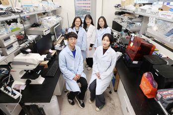
< Photo 1. (From top left) Professor Hyunjoo J. Lee, Dr. Mi-Young Son, Dr. Mi-Ok Lee (In the front row from left) Doctoral student Kiup Kim, Doctoral student Youngsun Lee > On January 14th, the KAIST research team led by Professor Hyunjoo J. Lee from the School of Electrical Engineering in collaboration with Dr. Mi-Young Son and Dr. Mi-Ok Lee at Korea Research Institute of Bioscience and Biotechnology (KRIBB) announced the development of a highly stretchable microelectrode array (sMEA) designed for non-invasive electrophysiological signal measurement of organoids. Organoids* are highly promising models for human biology and are expected to replace many animal experiments. Their potential applications include disease modeling, drug screening, and personalized medicine as they closely mimic the structure and function of humans. *Organoids: three-dimensional in vitro tissue models derived from human stem cells Despite these advantages, existing organoid research has primarily focused on genetic analysis, with limited studies on organoid functionality. For effective drug evaluation and precise biological research, technology that preserves the three-dimensional structure of organoids while enabling real-time monitoring of their functions is needed. However, it’s challenging to provide non-invasive ways to evaluate the functionalities without incurring damage to the tissues. This challenge is particularly significant for electrophysiological signal measurement in cardiac and brain organoids since the sensor needs to be in direct contact with organoids of varying size and irregular shape. Achieving tight contact between electrodes and the external surface of the organoids without damaging the organoids has been a persistent challenge. < Figure 1. Schematic image of highly stretchable MEA (sMEA) with protruding microelectrodes. > The KAIST research team developed a highly stretchable microelectrode array with a unique serpentine structure that contacts the surface of organoids in a highly conformal fashion. They successfully demonstrated real-time measurement and analysis of electrophysiological signals from two types of electrogenic organoids (heart and brain). By employing a micro-electromechanical system (MEMS)-based process, the team fabricated the serpentine-structured microelectrode array and used an electrochemical deposition process to develop PEDOT:PSS-based protruding microelectrodes. These innovations demonstrated exceptional stretchability and close surface adherence to various organoid sizes. The protruding microelectrodes improved contact between organoids and the electrodes, ensuring stable and reliable electrophysiological signal measurements with high signal-to-noise ratios (SNR). < Figure 2. Conceptual illustration, optical image, and fluorescence images of an organoid captured by the sMEA with protruding microelectrodes.> Using this technology, the team successfully monitored and analyzed electrophysiological signals from cardiac spheroids of various sizes, revealing three-dimensional signal propagation patterns and identifying changes in signal characteristics according to size. They also measured electrophysiological signals in midbrain organoids, demonstrating the versatility of the technology. Additionally, they monitored signal modulations induced by various drugs, showcasing the potential of this technology for drug screening applications. < Figure 3. SNR improvement effect by protruding PEDOT:PSS microelectrodes. > Prof. Hyunjoo Jenny Lee stated, “By integrating MEMS technology and electrochemical deposition techniques, we successfully developed a stretchable microelectrode array adaptable to organoids of diverse sizes and shapes. The high practicality is a major advantage of this system since the fabrication is based on semiconductor fabrication with high volume production, reliability, and accuracy. This technology that enables in situ, real-time analysis of states and functionalities of organoids will be a game changer in high-through drug screening.” This study led by Ph.D. candidate Kiup Kim from KAIST and Ph.D. candidate Youngsun Lee from KRIBB, with significant contributions from Dr. Kwang Bo Jung, was published online on December 15, 2024 in Advanced Materials (IF: 27.4). < Figure 4. Drug screening using cardiac spheroids and midbrain organoids.> This research was supported by a grant from 3D-TissueChip Based Drug Discovery Platform Technology Development Program (No. 20009209) funded by the Ministry of Trade, Industry & Energy (MOTIE, Korea), by the Commercialization Promotion Agency for R&D Outcomes (COMPA) funded by the Ministry of Science and ICT (MSIT) (RS-2024-00415902), by the K-Brain Project of the National Research Foundation (NRF) funded by the Korean government (MSIT) (RS-2023-00262568), by BK21 FOUR (Connected AI Education & Research Program for Industry and Society Innovation, KAIST EE, No. 4120200113769), and by Korea Research Institute of Bioscience and Biotechnology (KRIBB) Research Initiative Program (KGM4722432).
-
KAIST Develops CamBio - a New Biotemplating Method..
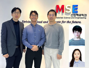
- Professor Jae-Byum Chang and Professor Yeon Sik Jung’s joint research team of the Department of Materials Science and Engineering developed a highly tunable bio-templating method “CamBio” that makes use of intracellular protein structures - Substrate performance improvement of up to 230% demonstrated via surface-enhanced Raman spectroscopy (SERS) - Expected to have price competitiveness over bio-templating method as it expands the range of biological samples - Expected to expand the range of application of nanostructure synthesis technology by utilizing various biological structures < Photo 1. (From left) Professor Yeon Sik Jung, Ph.D. candidate Dae-Hyeon Song, Professor Jae-Byum Chang, and (from top right) Dr. Chang Woo Song and Dr. Seunghee H. Cho of the Department of Materials Science and Engineering > Biological structures have complex characteristics that are difficult to replicate artificially, but biotemplating methods* that directly utilize these biological structures have been used in various fields of application. The KAIST research team succeeded in utilizing previously unusable biological structures and expanding the areas in which biotemplate methods can be applied. *Biotemplating: A method of using biotemplates as a mold to create functional structural materials, utilizing the functions of these biological structures, from viruses to the tissues and organs that make up our bodies KAIST (President Kwang Hyung Lee) announced on the 10th that a joint research team of Professors Jae-Byum Chang and Professor Yeon Sik Jung of the Department of Materials Science and Engineering developed a biotemplating method that utilizes specific intracellular proteins in biological samples and has high tunability. Existing biotemplate methods mainly utilize only the external surface of biological samples or have limitations in utilizing the structure-function correlation of various biological structures due to limited dimensions and sample sizes, making it difficult to create functional nanostructures. To solve this problem, the research team studied a way to utilize various biological structures within the cells while retaining high tunability. < Figure 1. CamBio utilizing microtubules, a intracellular protein structure. The silver nanoparticle chains synthesized along the microtubules that span the entire cell interior can be observed through an electron microscope, and it is shown that this can be used as a successful SERS substrate. > As a result of the research, the team developed the “Conversion to advanced materials via labeled Biostructure”, shortened as “CamBio”, which enables the selective synthesis of nanostructures with various characteristics and sizes from specific protein structures composed of diverse proteins within biological specimens. The CamBio method secures high tunability of functional nanostructures that can be manufactured from biological samples by merging various manufacturing and biological technologies. Through the technology of repeatedly attaching antibodies, arranging cells in a certain shape, and thinly slicing tissue, the functional nanostructures made with CamBio showed improved performance on the surface-enhanced Raman spectroscopy (SERS)* substrate used for material detection. *Surface-enhanced Raman spectroscopy (SERS): A technology that can detect very small amounts of substances using light, based on the principle that specific substances react to light and amplifies signals on surfaces of metals such as gold or silver. The research team found that the nanoparticle chains made using the intracellular protein structures through the process of repeated labeling with antibodies allowed easier control, and improved SERS performance by up to 230%. In addition, the research team expanded from utilizing the structures inside cells to obtaining samples of muscle tissues inside meat using a cryostat and successfully producing a substrate with periodic bands made of metal particles by performing the CamBio process. This method of producing a substrate not only allows large-scale production using biological samples, but also shows that it is a cost-effective method. < Figure 2. A method for securing tunability using CamBio at the cell level. Examples of controlling characteristics by integrating iterative labeling and cell pattering techniques with CamBio are shown. > The CamBio developed by the research team is expected to be used as a way to solve problems faced by various research fields as it is to expand the range of bio-samples that can be produced for various usage. The first author, Dae-Hyeon Song, a Ph.D. candidate of KAIST Department of Materials Science and Engineering said, “Through CamBio, we have comprehensively accumulated biotemplating methods that can utilize more diverse protein structures,” and “If combined with the state-of-the-art biological technologies such as gene editing and 3D bioprinting and new material synthesis technologies, biostructures can be utilized in various fields of application.” < Figure 3. A method for securing tunability using CamBio at the tissue level. In order to utilize proteins inside muscle tissue, the frozen tissue sectioning technology is combined, and through this, a substrate with a periodic nanoparticle band pattern is successfully produced, and it is shown that large-area acquisition of samples and price competitiveness can be achieved. > This study, in which the Ph.D. candidate Dae-Hyeon Song along with Dr. Chang Woo Song, and Dr. Seunghee H. Cho of the same department participated as the first authors, was published online in the international academic journal, Advanced Science, on November 13th, 2024. (Paper title: Highly Tunable, Nanomaterial-Functionalized Structural Templating of Intracellular Protein Structures Within Biological Species) https://doi.org/10.1002/advs.202406492 This study was conducted with a combination of support from various programs including the National Convergence Research of Scientific Challenges (National Research Foundation of Korea (NRF) 2024), Engineering Reseach Center (ERC) (Wearable Platform Materials Technology Center, NRF 2023), ERC (Global Bio-integrated Materials Center, NRF 2024), and the National Advanced Program for Biological Research Resources (Bioimaging Data Curation Center, NRF 2024) funded by Ministry of Science and ICT.

291 Daehak-ro, Yuseong-gu, Daejeon, Korea 34141
KAIST College of Engineering
T.+82-42-350-2114
F.+82-42-350-2210 (2220)
ⓒ KAIST College of Engineering. All rights reserved.