


Students News
-
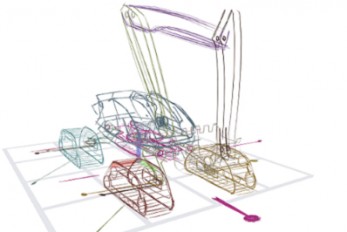
“3D sketch” Your Ideas and Bring Them to Life, Ins..
Professor Seok-Hyung Bae’s research team at the Department of Industrial Design developed a novel 3D sketching system that rapidly creates animated 3D concepts through simple user interactions like sketching on a piece of paper or playing a toy. Foldable drones, transforming vehicles, and multi-legged robots from sci-fi movies are now becoming commonplace thanks to technological progress. However, designing them remains a difficult challenge even for skilled experts, because complex design decisions must be made regarding not only their form, but also the structure, poses, and motions, which are interdependent on one another. Creating a 3D concept comprising of multiple moving parts connected by different types of joints using a traditional 3D CAD tool, which is more suited for processing precise and elaborate modeling, is a painstaking and time-consuming process. This presents a major bottleneck for the workflow during the early stage of design, in which it is preferred that as many ideas are tried and discarded out as quickly as possible in order to explore a wide range of possibilities in the shortest amount of time. A research team led by Professor Bae has focused on designers’ freehand sketches drew up with a pen on a paper that serve as the starting point for virtually all design projects. This led them to develop their 3D sketching technology to generate desired 3D curves from the rough but expressive 2D strokes drawn with a digital stylus on a digital tablet. Their latest research helps designers bring their 3D sketches to life almost instantly. Using the intuitive set of multi-touch gestures the team successfully designed and implemented, designers can handle the 3D sketches they are working on with their fingers as if they are playing with toys and put them into animation in no time. < Figure 1. A novel 3D sketching system for rapidly designing articulated 3D concepts with a small set of coherent pen and multi-touch gestures. (a) Sketching: A 3D sketch curve is created by marking a pen stroke that is projected onto a sketch plane widget. (b) Segmenting: Entire or partial sketch curves are added to separate parts that serve as links in the kinematic chain. (c) Rigging: Repeatedly demonstrating the desired motion of a part leaves behind a trail, from which the system infers a joint. (d) Posing: Desired poses can be achieved through actuating joints via forward or inverse kinematics. (e) Filming: A sequence of keyframes specifying desired poses and viewpoints is connected as a smooth motion. > < Figure 2. (a) Concept drawing of an autonomous excavator. It features (b, c) four caterpillars that swivel for high maneuverability, (d) an extendable boom and a bucket connected by multiple links, and (e) a rotating platform. The concept’s designer, who had 8 years of work experience, estimated that it would take 1-2 weeks to express and communicate such a complex articulated object with existing tools. With the proposed system, it took only 2 hours and 52 minutes. > The major findings of their work were published under the title “Rapid Design of Articulated Objects” in ACM Transactions on Graphics (impact factor: 7.403), the top international journal in the field of computer graphics, and presented at ACM SIGGRAPH 2022 (h5-index: 103), the world’s largest international academic conference in the field, which was held back in August in Vancouver, Canada with Joon Hyub Lee, a Ph.D. student of the Department of Industrial Design as the first author. The ACM SIGGRAPH 2022 conference was reportedly attended by over 10,000 participants including researchers, artists, and developers from world-renowned universities; film, animation, and game studies, such as Marvel, Pixar, and Blizzard; high-tech manufacturers, such as Lockheed Martin and Boston Dynamics; and metaverse platform companies, such as Meta and Roblox. < Figure 3. The findings of Professor Bae’s research team were published in ACM Transactions on Graphics, the top international academic journal in the field of computer graphics, and presented at ACM SIGGRAPH 2022, the largest international academic conference held in conjunction early August in Vancouver, Canada. The team’s live demo at the Emerging Technologies program was highly praised by numerous academics and industry officials and received an Honorable Mention. > The team was also invited to present their technical paper as a demo and a special talk at the Emerging Technologies program at ACM SIGGRAPH 2022 as one of the top-three impactful technologies. The live performance, in which Hanbit Kim, a Ph.D. student of the Department of Industrial Design at KAIST and a co-author, sketched and animated a sophisticated animal-shaped robot from scratch in a matter of a few minutes, wowed the audience and won the Honorable Mention Award from the jury. Edwin Catmull, the co-founder of Pixar and a keynote speaker at the SIGGRAPH conference, praised the team’s research on 3D sketching as “really excellent work” and “a kind of tool that would be useful to Pixar's creative model designers.” This technology, which became virally popular in Japan after featuring in an online IT media outlet and attracting more than 600K views, received a special award from the Digital Content Association of Japan (DCAJ) and was invited and exhibited for three days at Tokyo in November, as a part of Inter BEE 2022, the largest broadcasting and media expo in Japan. “The more we come to understand how designers think and work, the more effective design tools can be built around that understanding,” said Professor Bae, explaining that “the key is to integrate different algorithms into a harmonious system as intuitive interactions.” He added that “this work wouldn’t have been possible if it weren’t for the convergent research environment cultivated by the Department of Industrial Design at KAIST, in which all students see themselves not only as aspiring creative designers, but also as practical engineers.” By enabling designers to produce highly expressive animated 3D concepts far more quickly and easily in comparison to using existing methods, this new tool is expected to revolutionize design practices and processes in the content creation, manufacturing, and metaverse-related industries. This research was funded by the Ministry of Science and ICT, and the National Research Foundation of Korea. More info: https://sketch.kaist.ac.kr/publications/2022_siggraph_rapid_design Video: https://www.youtube.com/watch?v=rsBl0QvSDqI < Figure 4. From left to right: Ph.D. students Hanbit Kim, and Joon Hyub Lee and Professor Bae of the Department of Industrial Design, KAIST >
-

Metabolically Engineered Bacterium Produces Lutein..
A research group at KAIST has engineered a bacterial strain capable of producing lutein. The research team applied systems metabolic engineering strategies, including substrate channeling and electron channeling, to enhance the production of lutein in an engineered Escherichia coli strain. The strategies will be also useful for the efficient production of other industrially important natural products used in the food, pharmaceutical, and cosmetic industries. Figure: Systems metabolic engineering was employed to construct and optimize the metabolic pathways for lutein production, and substrate channeling and electron channeling strategies were additionally employed to increase the production of the lutein with high productivity. Lutein is classified as a xanthophyll chemical that is abundant in egg yolk, fruits, and vegetables. It protects the eye from oxidative damage from radiation and reduces the risk of eye diseases including macular degeneration and cataracts. Commercialized products featuring lutein are derived from the extracts of the marigold flower, which is known to harbor abundant amounts of lutein. However, the drawback of lutein production from nature is that it takes a long time to grow and harvest marigold flowers. Furthermore, it requires additional physical and chemical-based extractions with a low yield, which makes it economically unfeasible in terms of productivity. The high cost and low yield of these bioprocesses has made it difficult to readily meet the demand for lutein. These challenges inspired the metabolic engineers at KAIST, including researchers Dr. Seon Young Park, Ph.D. Candidate Hyunmin Eun, and Distinguished Professor Sang Yup Lee from the Department of Chemical and Biomolecular Engineering. The team’s study entitled “Metabolic engineering of Escherichia coli with electron channeling for the production of natural products” was published in Nature Catalysis on August 5, 2022. This research details the ability to produce lutein from E. coli with a high yield using a cheap carbon source, glycerol, via systems metabolic engineering. The research group focused on solving the bottlenecks of the biosynthetic pathway for lutein production constructed within an individual cell. First, using systems metabolic engineering, which is an integrated technology to engineer the metabolism of a microorganism, lutein was produced when the lutein biosynthesis pathway was introduced, albeit in very small amounts. To improve the productivity of lutein production, the bottleneck enzymes within the metabolic pathway were first identified. It turned out that metabolic reactions that involve a promiscuous enzyme, an enzyme that is involved in two or more metabolic reactions, and electron-requiring cytochrome P450 enzymes are the main bottleneck steps of the pathway inhibiting lutein biosynthesis. To overcome these challenges, substrate channeling, a strategy to artificially recruit enzymes in physical proximity within the cell in order to increase the local concentrations of substrates that can be converted into products, was employed to channel more metabolic flux towards the target chemical while reducing the formation of unwanted byproducts. Furthermore, electron channeling, a strategy similar to substrate channeling but differing in terms of increasing the local concentrations of electrons required for oxidoreduction reactions mediated by P450 and its reductase partners, was applied to further streamline the metabolic flux towards lutein biosynthesis, which led to the highest titer of lutein production achieved in a bacterial host ever reported. The same electron channeling strategy was successfully applied for the production of other natural products including nootkatone and apigenin in E. coli, showcasing the general applicability of the strategy in the research field. “It is expected that this microbial cell factory-based production of lutein will be able to replace the current plant extraction-based process,” said Dr. Seon Young Park, the first author of the paper. She explained that another important point of the research is that integrated metabolic engineering strategies developed from this study can be generally applicable for the efficient production of other natural products useful as pharmaceuticals or nutraceuticals. “As maintaining good health in an aging society is becoming increasingly important, we expect that the technology and strategies developed here will play pivotal roles in producing other valuable natural products of medical or nutritional importance,” explained Distinguished Professor Sang Yup Lee. This work was supported by the Cooperative Research Program for Agriculture Science & Technology Development funded by the Rural Development Administration of Korea, with further support from the Development of Next-generation Biorefinery Platform Technologies for Leading Bio-based Chemicals Industry Project and by the Development of Platform Technologies of Microbial Cell Factories for the Next-generation Biorefineries Project of the National Research Foundation funded by the Ministry of Science and ICT of Korea.
-

A System for Stable Simultaneous Communication amo..
A mmWave Backscatter System, developed by a team led by Professor Song Min Kim is exciting news for the IoT market as it will be able to provide fast and stable connectivity even for a massive network, which could finally allow IoT devices to reach their full potential. A research team led by Professor Song Min Kim of the KAIST School of Electrical Engineering developed a system that can support concurrent communications for tens of millions of IoT devices using backscattering millimeter-level waves (mmWave). With their mmWave backscatter method, the research team built a design enabling simultaneous signal demodulation in a complex environment for communication where tens of thousands of IoT devices are arranged indoors. The wide frequency range of mmWave exceeds 10GHz, which provides great scalability. In addition, backscattering reflects radiated signals instead of wirelessly creating its own, which allows operation at ultralow power. Therefore, the mmWave backscatter system offers internet connectivity on a mass scale to IoT devices at a low installation cost. This research by Kangmin Bae et al. was presented at ACM MobiSys 2022. At this world-renowned conference for mobile systems, the research won the Best Paper Award under the title “OmniScatter: Sensitivity mmWave Backscattering Using Commodity FMCW Radar”. It is meaningful that members of the KAIST School of Electrical Engineering have won the Best Paper Award at ACM MobiSys for two consecutive years, as last year was the first time the award was presented to an institute from Asia. IoT, as a core component of 5G/6G network, is showing exponential growth, and is expected to be part of a trillion devices by 2035. To support the connection of IoT devices on a mass scale, 5G and 6G each aim to support ten times and 100 times the network density of 4G, respectively. As a result, the importance of practical systems for large-scale communication has been raised. The mmWave is a next-generation communication technology that can be incorporated in 5G/6G standards, as it utilizes carrier waves at frequencies between 30 to 300GHz. However, due to signal reduction at high frequencies and reflection loss, the current mmWave backscatter system enables communication in limited environments. In other words, it cannot operate in complex environments where various obstacles and reflectors are present. As a result, it is limited to the large-scale connection of IoT devices that require a relatively free arrangement. The research team found the solution in the high coding gain of an FMCW radar. The team developed a signal processing method that can fundamentally separate backscatter signals from ambient noise while maintaining the coding gain of the radar. They achieved a receiver sensitivity of over 100 thousand times that of previously reported FMCW radars, which can support communication in practical environments. Additionally, given the radar’s property where the frequency of the demodulated signal changes depending on the physical location of the tag, the team designed a system that passively assigns them channels. This lets the ultralow-power backscatter communication system to take full advantage of the frequency range at 10 GHz or higher. The developed system can use the radar of existing commercial products as gateway, making it easily compatible. In addition, since the backscatter system works at ultralow power levels of 10uW or below, it can operate for over 40 years with a single button cell and drastically reduce installation and maintenance costs. The research team confirmed that mmWave backscatter devices arranged randomly in an office with various obstacles and reflectors could communicate effectively. The team then took things one step further and conducted a successful trace-driven evaluation where they simultaneously received information sent by 1,100 devices. Their research presents connectivity that greatly exceeds network density required by next-generation communication like 5G and 6G. The system is expected to become a stepping stone for the hyper-connected future to come. Professor Kim said, “mmWave backscatter is the technology we’ve dreamt of. The mass scalability and ultralow power at which it can operate IoT devices is unmatched by any existing technology”. He added, “We look forward to this system being actively utilized to enable the wide availability of IoT in the hyper-connected generation to come”. To demonstrate the massive connectivity of the system, a trace-driven evaluation of 1,100 concurrent tag transmissions are made. Figure shows the demodulation result of each and every 1,100 tags as red triangles, where they successfully communicate without collision. This work was supported by Samsung Research Funding & Incubation Center of Samsung Electronics and by the ITRC (Information Technology Research Center) support program supervised by the IITP (Institute of Information & Communications Technology Planning & Evaluation). Profile: Song Min Kim, Ph.D. Professor songmin@kaist.ac.kr https://smile.kaist.ac.kr SMILE Lab. School of Electrical Engineering
-

An AI-based, Indoor/Outdoor-Integrated (IOI) GPS S..
KAIST breaks new grounds in positioning technology with an AI-integrated GPS board that works both indoors and out KAIST (President Kwang Hyung Lee) announced on the 8th that Professor Dong-Soo Han's research team (Intelligent Service Integration Lab) from the School of Computing has developed a GPS system that works both indoors and outdoors with quality precision regardless of the environment. This Indoor/Outdoor-Integrated GPS System, or IOI GPS System, for short, uses the GPS signals outdoors and estimates locations indoors using signals from multiple sources like an inertial sensor, pressure sensors, geomagnetic sensors, and light sensors. To this end, the research team developed techniques to detect environmental changes such as entering a building, and methods to detect entrances, ground floors, stairs, elevators and levels of buildings by utilizing artificial intelligence techniques. Various landmark detecting techniques were also incorporated with pedestrian dead reckoning (PDR), a navigation tool for pedestrians, to devise the so-called “Sensor-Fusion Positioning Algorithm”. To date, it was common to estimate locations based on wireless LAN signals or base station signals in a space where the GPS signal could not reach. However, the IOI GPS enables positioning even in buildings without signals nor indoor maps. The algorithm developed by the research team can provide accurate floor information within a building where even big tech companies like Google and Apple's positioning services do not provide. Unlike other positioning methods that rely on visual data, geomagnetic positioning techniques, or wireless LAN, this system also has the advantage of not requiring any prior preparation. In other words, the foundation to enable the usage of a universal GPS system that works both indoors and outdoors anywhere in the world is now ready. The research team also produced a circuit board for the purpose of operating the IOI GPS System, mounted with chips to receive and process GPS, Wi-Fi, and Bluetooth signals, along with an inertial sensor, a barometer, a magnetometer, and a light sensor. The sensor-fusion positioning algorithm the lab has developed is also incorporated in the board. When the accuracy of the IOI GPS board was tested in the N1 building of KAIST’s main campus in Daejeon, it achieved an accuracy of about 95% in floor estimation and an accuracy of about 3 to 6 meters in distance estimation. As for the indoor/outdoor transition, the navigational mode change was completed in about 0.3 seconds. When it was combined with the PDR technique, the estimation accuracy improved further down to a scope of one meter. The research team is now working on assembling a tag with a built-in positioning board and applying it to location-based docent services for visitors at museums, science centers, and art galleries. The IOI GPS tag can be used for the purpose of tracking children and/or the elderly, and it can also be used to locate people or rescue workers lost in disaster-ridden or hazardous sites. On a different note, the sensor-fusion positioning algorithm and positioning board for vehicles are also under development for the tracking of vehicles entering indoor areas like underground parking lots. When the IOI GPS board for vehicles is manufactured, the research team will work to collaborate with car manufacturers and car rental companies, and will also develop a sensor-fusion positioning algorithm for smartphones. Telecommunication companies seeking to diversify their programs in the field of location-based services will also be interested in the use the IOI GPS. Professor Dong-Soo Han of the School of Computing, who leads the research team, said, “This is the first time to develop an indoor/outdoor integrated GPS system that can pinpoint locations in a building where there is no wireless signal or an indoor map, and there are an infinite number of areas it can be applied to. When the integration with the Korea Augmentation Satellite System (KASS) and the Korean GPS (KPS) System that began this year, is finally completed, Korea can become the leader in the field of GPS both indoors and outdoors, and we also have plans to manufacture semi-conductor chips for the IOI GPS System to keep the tech-gap between Korea and the followers.” He added, "The guidance services at science centers, museums, and art galleries that uses IOI GPS tags can provide a set of data that would be very helpful for analyzing the visitors’ viewing traces. It is an essential piece of information required when the time comes to decide when to organize the next exhibit. We will be working on having it applied to the National Science Museum, first.” The projects to develop the IOI GPS system and the trace analysis system for science centers were supported through Science, Culture, Exhibits and Services Capability Enhancement Program of the Ministry of Science and ICT. Profile: Dong-Soo Han, Ph.D. Professor ddsshhan@kaist.ac.kr http://isilab.kaist.ac.kr Intelligent Service Integration Lab. School of Computing http://kaist.ac.kr/en/ Korea Advanced Institute of Science and Technology (KAIST) Daejeon, Republic of Korea
-

Interactive Map of Metabolical Synthesis of Chemic..
An interactive map that compiled the chemicals produced by biological, chemical and combined reactions has been distributed on the web - A team led by Distinguished Professor Sang Yup Lee of the Department of Chemical and Biomolecular Engineering, organized and distributed an all-inclusive listing of chemical substances that can be synthesized using microorganisms - It is expected to be used by researchers around the world as it enables easy assessment of the synthetic pathway through the web. A research team comprised of Woo Dae Jang, Gi Bae Kim, and Distinguished Professor Sang Yup Lee of the Department of Chemical and Biomolecular Engineering at KAIST reported an interactive metabolic map of bio-based chemicals. Their research paper “An interactive metabolic map of bio-based chemicals” was published online in Trends in Biotechnology on August 10, 2022. As a response to rapid climate change and environmental pollution, research on the production of petrochemical products using microorganisms is receiving attention as a sustainable alternative to existing methods of productions. In order to synthesize various chemical substances, materials, and fuel using microorganisms, it is necessary to first construct the biosynthetic pathway toward desired product by exploration and discovery and introduce them into microorganisms. In addition, in order to efficiently synthesize various chemical substances, it is sometimes necessary to employ chemical methods along with bioengineering methods using microorganisms at the same time. For the production of non-native chemicals, novel pathways are designed by recruiting enzymes from heterologous sources or employing enzymes designed though rational engineering, directed evolution, or ab initio design. The research team had completed a map of chemicals which compiled all available pathways of biological and/or chemical reactions that lead to the production of various bio-based chemicals back in 2019 and published the map in Nature Catalysis. The map was distributed in the form of a poster to industries and academia so that the synthesis paths of bio-based chemicals could be checked at a glance. The research team has expanded the bio-based chemicals map this time in the form of an interactive map on the web so that anyone with internet access can quickly explore efficient paths to synthesize desired products. The web-based map provides interactive visual tools to allow interactive visualization, exploration, and analysis of complex networks of biological and/or chemical reactions toward the desired products. In addition, the reported paper also discusses the production of natural compounds that are used for diverse purposes such as food and medicine, which will help designing novel pathways through similar approaches or by exploiting the promiscuity of enzymes described in the map. The published bio-based chemicals map is also available at http://systemsbiotech.co.kr. The co-first authors, Dr. Woo Dae Jang and Ph.D. student Gi Bae Kim, said, “We conducted this study to address the demand for updating the previously distributed chemicals map and enhancing its versatility.” “The map is expected to be utilized in a variety of research and in efforts to set strategies and prospects for chemical production incorporating bio and chemical methods that are detailed in the map.” Distinguished Professor Sang Yup Lee said, “The interactive bio-based chemicals map is expected to help design and optimization of the metabolic pathways for the biosynthesis of target chemicals together with the strategies of chemical conversions, serving as a blueprint for developing further ideas on the production of desired chemicals through biological and/or chemical reactions.” The interactive metabolic map of bio-based chemicals.
-

PICASSO Technique Drives Biological Molecules into..
The new imaging approach brings current imaging colors from four to more than 15 for mapping overlapping proteins Pablo Picasso’s surreal cubist artistic style shifted common features into unrecognizable scenes, but a new imaging approach bearing his namesake may elucidate the most complicated subject: the brain. Employing artificial intelligence to clarify spectral color blending of tiny molecules used to stain specific proteins and other items of research interest, the PICASSO technique, allows researchers to use more than 15 colors to image and parse our overlapping proteins. The PICASSO developers, based in Korea, published their approach on May 5 in Nature Communications. < 45-color multiplexed imaging of the mouse hippocampus via PICASSO in three staining and imaging rounds (Nature Communications/KAIST) > Fluorophores — the staining molecules — emit specific colors when excited by a light, but if more than four fluorophores are used, their emitted colors overlap and blend. Researchers previously developed techniques to correct this spectral overlap by precisely defining the matrix of mixed and unmixed images. This measurement depends on reference spectra, found by identifying clear images of only one fluorophore-stained specimen or of multiple, identically prepared specimens that only contain a single fluorophore each. “Such reference spectra measurement could be complicated to perform in highly heterogeneous specimens, such as the brain, due to the highly varied emission spectra of fluorophores depending on the subregions from which the spectra were measured,” said co-corresponding author Young-Gyu Yoon, professor in the School of Electrical Engineering at KAIST. He explained that the subregions would each need their own spectra reference measurements, making for an inefficient, time-consuming process. “To address this problem, we developed an approach that does not require reference spectra measurements.” The approach is the “Process of ultra-multiplexed Imaging of biomolecules viA the unmixing of the Signals of Spectrally Overlapping fluorophores,” also known as PICASSO. Ultra-multiplexed imaging refers to visualizing the numerous individual components of a unit. Like a cinema multiplex in which each theater plays a different movie, each protein in a cell has a different role. By staining with fluorophores, researchers can begin to understand those roles. “We devised a strategy based on information theory; unmixing is performed by iteratively minimizing the mutual information between mixed images,” said co-corresponding author Jae-Byum Chang, professor in the Department of Materials Science and Engineering, KAIST. “This allows us to get away with the assumption that the spatial distribution of different proteins is mutually exclusive and enables accurate information unmixing.” To demonstrate PICASSO’s capabilities, the researchers applied the technique to imaging a mouse brain. With a single round of staining, they performed 15-color multiplexed imaging of a mouse brain. Although small, mouse brains are still complex, multifaceted organs that can take significant resources to map. According to the researchers, PICASSO can improve the capabilities of other imaging techniques and allow for the use of even more fluorophore colors. Using one such imaging technique in combination with PICASSO, the team achieved 45-color multiplexed imaging of the mouse brain in only three staining and imaging cycles, according to Yoon. “PICASSO is a versatile tool for the multiplexed biomolecule imaging of cultured cells, tissue slices and clinical specimens,” Chang said. “We anticipate that PICASSO will be useful for a broad range of applications for which biomolecules’ spatial information is important. One such application the tool would be useful for is revealing the cellular heterogeneities of tumor microenvironments, especially the heterogeneous populations of immune cells, which are closely related to cancer prognoses and the efficacy of cancer therapies.” The Samsung Research Funding & Incubation Center for Future Technology supported this work. Spectral imaging was performed at the Korea Basic Science Institute Western Seoul Center. -Publication Junyoung Seo, Yeonbo Sim, Jeewon Kim, Hyunwoo Kim, In Cho, Hoyeon Nam, Yong-Gyu Yoon, Jae-Byum Chang, “PICASSO allows ultra-multiplexed fluorescence imaging of spatially overlapping proteins without reference spectra measurements,” May 5, Nature Communications (doi.org/10.1038/s41467-022-30168-z) -Profile Professor Jae-Byum Chang Department of Materials Science and Engineering College of Engineering KAIST Professor Young-Gyu Yoon School of Electrical Engineering College of Engineering KAIST
-

Professor Juho Kim’s Team Wins Best Paper Award at..
The research team led by Professor Juho Kim from the KAIST School of Computing won a Best Paper Award and an Honorable Mention Award at the Association for Computing Machinery Conference on Human Factors in Computing Systems (ACM CHI) held between April 30 and May 6. ACM CHI is the world’s most recognized conference in the field of human computer interactions (HCI), and is ranked number one out of all HCI-related journals and conferences based on Google Scholar’s h-5 index. Best paper awards are given to works that rank in the top one percent, and honorable mention awards are given to the top five percent of the papers accepted by the conference. Professor Juho Kim presented a total of seven papers at ACM CHI 2022, and tied for the largest number of papers. A total of 19 papers were affiliated with KAIST, putting it fifth out of all participating institutes and thereby proving KAIST’s competence in research. < From left: MS graduate Jeongyeon Kim from the School of Computing, MS candidate Yubin Choi from the School of Electrical Engineering, and Dr. Meng Xia, and Professor Kim > One of Professor Kim’s research teams composed of Jeongyeon Kim (first author, MS graduate) from the School of Computing, MS candidate Yubin Choi from the School of Electrical Engineering, and Dr. Meng Xia (post-doctoral associate in the School of Computing, currently a post-doctoral associate at Carnegie Mellon University) received a best paper award for their paper, “Mobile-Friendly Content Design for MOOCs: Challenges, Requirements, and Design Opportunities”. The study analyzed the difficulties experienced by learners watching video-based educational content in a mobile environment and suggests guidelines for solutions. The research team analyzed 134 survey responses and 21 interviews, and revealed that texts that are too small or overcrowded are what mainly brings down the legibility of video contents. Additionally, lighting, noise, and surrounding environments that change frequently are also important factors that may disturb a learning experience. Based on these findings, the team analyzed the aptness of 41,722 frames from 101 video lectures for mobile environments, and confirmed that they generally show low levels of adequacy. For instance, in the case of text sizes, only 24.5% of the frames were shown to be adequate for learning in mobile environments. To overcome this issue, the research team suggested a guideline that may improve the legibility of video contents and help overcome the difficulties arising from mobile learning environments. The importance of and dependency on video-based learning continue to rise, especially in the wake of the pandemic, and it is meaningful that this research suggested a means to analyze and tackle the difficulties of users that learn from the small screens of mobile devices. Furthermore, the paper also suggested technology that can solve problems related to video-based learning through human-AI collaborations, enhancing existing video lectures and improving learning experiences. This technology can be applied to various video-based platforms and content creation. < From left: Ph.D. candidate Tae Soo Kim, MS candidate DaEun Choi, and Ph.D. candidate Yoonseo Choi, and Professor Kim > Meanwhile, a research team composed of Ph.D. candidate Tae Soo Kim (first author), MS candidate DaEun Choi, and Ph.D. candidate Yoonseo Choi from the School of Computing received an honorable mention award for their paper, “Stylette: styling the Web with Natural Language”. The research team developed a novel interface technology that allows nonexperts who are unfamiliar with technical jargon to edit website features through speech. People often find it difficult to use or find the information they need from various websites due to accessibility issues, device-related constraints, inconvenient design, style preferences, etc. However, it is not easy for laymen to edit website features without expertise in programming or design, and most end up just putting up with the inconveniences. But what if the system could read the intentions of its users from their everyday language like “emphasize this part a little more”, or “I want a more modern design”, and edit the features automatically? Based on this question, Professor Kim’s research team developed ‘Stylette’, a system in which AI analyses its users’ speech expressed in their natural language and automatically recommends a new style that best fits their intentions. The research team created a new system by putting together language AI, visual AI, and user interface technologies. On the linguistic side, a large-scale language model AI converts the intentions of the users expressed through their everyday language into adequate style elements. On the visual side, computer vision AI compares 1.7 million existing web design features and recommends a style adequate for the current website. In an experiment where 40 nonexperts were asked to edit a website design, the subjects that used this system showed double the success rate in a time span that was 35% shorter compared to the control group. It is meaningful that this research proposed a practical case in which AI technology constructs intuitive interactions with users. The developed technology can be applied to existing design applications and web browsers in a plug-in format, and can be utilized to improve websites or for advertisements by collecting the natural intention data of users on a large scale.
-

Now You Can See Floral Scents!
Optical interferometry visualizes how often lilies emit volatile organic compounds < Image: Direct measurement of floral scents from a live lily using a laser interferometry method. The signal of the refractive index difference was monitored and the VOCs’ emission frequency results were calculated from Fast Fourier Transform. It showed the unsteady VOC emissions. > Have you ever thought about when flowers emit their scents? KAIST mechanical engineers and biological scientists directly visualized how often a lily releases a floral scent using a laser interferometry method. These measurement results can provide new insights for understanding and further exploring the biosynthesis and emission mechanisms of floral volatiles. Why is it important to know this? It is well known that the fragrance of flowers affects their interactions with pollinators, microorganisms, and florivores. For instance, many flowering plants can tune their scent emission rates when pollinators are active for pollination. Petunias and the wild tobacco Nicotiana attenuata emit floral scents at night to attract night-active pollinators. Thus, visualizing scent emissions can help us understand the ecological evolution of plant-pollinator interactions. Many groups have been trying to develop methods for scent analysis. Mass spectrometry has been one widely used method for investigating the fragrance of flowers. Although mass spectrometry reveals the quality and quantity of floral scents, it is impossible to directly measure the releasing frequency. A laser-based gas detection system and a smartphone-based detection system using chemo-responsive dyes have also been used to measure volatile organic compounds (VOCs) in real-time, but it is still hard to measure the time-dependent emission rate of floral scents. However, the KAIST research team co-led by Professor Hyoungsoo Kim from the Department of Mechanical Engineering and Professor Sang-Gyu Kim from the Department of Biological Sciences measured a refractive index difference between the vapor of the VOCs of lilies and the air to measure the emission frequency. The floral scent vapor was detected and the refractive index of air was 1.0 while that of the major floral scent of a linalool lily was 1.46. Professor Hyoungsoo Kim said, “We expect this technology to be further applicable to various industrial sectors such as developing it to detect hazardous substances in a space.” The research team also plans to identify the DNA mechanism that controls floral scent secretion. The current work entitled “Real-time visualization of scent accumulation reveals the frequency of floral scent emissions” was published in ‘Frontiers in Plant Science’ on April 18, 2022. (https://doi.org/10.3389/fpls.2022.835305). This research was supported by the Basic Science Research Program through the National Research Foundation of Korea (NRF-2021R1A2C2007835), the Rural Development Administration (PJ016403), and the KAIST-funded Global Singularity Research PREP-Program. -Publication: H. Kim, G. Lee, J. Song, and S.-G. Kim, "Real-time visualization of scent accumulation reveals the frequency of floral scent emissions," Frontiers in Plant Science 18, 835305 (2022) (https://doi.org/10.3389/fpls.2022.835305) -Profile: Professor Hyoungsoo Kim http://fil.kaist.ac.kr @MadeInH on Twitter Department of Mechanical Engineering KAIST Professor Sang-Gyu Kim https://sites.google.com/view/kimlab/home Department of Biological Sciences KAIST
-

Professor Sang Su Lee’s Team Wins Seven iF Design ..
Professor Sang Su Lee from the Department of Industrial Design and his team’s five apps made in collaboration with NH Investment and Securities won iF Design Awards in the fields of UI, UX, service design, product design, and communication. These apps are now offered as NH Investment and Securities mobile applications. The iF Design Awards recognize top quality creativity in product design, communication, packaging, service design and concepts, and architecture and interior design, as well as user experience (UX) and interface for digital media (UI). In the field of UI, ‘Gretell’ is a mobile stock investment app service designed by Lee and his team to support investors struggling to learn about investing by archiving personalized information. Gretell provides investment information including news and reports. Users learn, evaluate, and leave comments. This shows both quantitative and qualitative indications, leading to rational decision-making. Other user’s comments are shared to reduce confirmation bias. Through this process, Gretell helps users who are impulsive or easily swayed by others’ opinions to grow as independent investors. ‘Bright’ is another app created by Lee’s team. It helps people exercise their rights as shareholders. As the need to exercise shareholders’ rights increases, many people are frustrated that investors with a small number of shares don’t have a lot of power. Bright provides a space for shareholders to share their opinions and brings people together so that individuals can be more proactive as shareholders. The Integrated Power of Attorney System (IPAS) expands the chances for shareholders to exercise their rights and allows users to submit proposals that can be communicated during the general meeting. Bright fosters influential shareholders, responsible companies, and a healthy society. For communications, ‘Rewind’ is a stock information services app that visualizes past stock charts through sentiment analysis. Existing services focus on numbers, while Rewind takes a qualitative approach. Rewind analyzes public sentiment toward each event by collecting opinions on social media and then visualizes them chronologically along with the stock chart. Rewind allows users to review stock market movements and record their thoughts. Users can gain their own insights into current events in the stock market and make wiser investment decisions. The intuitive color gradient design provides a pleasant and simplified information experience. In the area of interfaces for digital media and service design, ‘Groo’ is a green bond investing service app that helps users participate in green investment though investing in green bonds that support green projects for environmental improvement. Not restricted to trading bonds, Groo joins users in the holistic experience of green investing, from taking an interest in environmental issues to confirming the impact of the investment. Next, ‘Modu’ is a story-based empathy expression training game for children with intellectual disabilities. Modu was developed to support emotion recognition and empathy behavior training in children with mild intellectual disabilities (MID) and borderline intellectual functioning (BIF). Finally, the diving VR device for neutral buoyancy training, ‘Blow-yancy’, also made winner’s list. The device mimics scuba diving training without having to go into the water, therefore beginner divers are able getting feeling of diving while remaining perfectly safe and not harming any corals. It is expected that the device will be able to help protect at-risk underwater ecosystems.
-

A New Strategy for Active Metasurface Design Provi..
The new strategy displays an unprecedented upper limit of dynamic phase modulation with no significant variations in optical amplitude An international team of researchers led by Professor Min Seok Jang of KAIST and Professor Victor W. Brar of the University of Wisconsin-Madison has demonstrated a widely applicable methodology enabling a full 360° active phase modulation for metasurfaces while maintaining significant levels of uniform light amplitude. This strategy can be fundamentally applied to any spectral region with any structures and resonances that fit the bill. Metasurfaces are optical components with specialized functionalities indispensable for real-life applications ranging from LIDAR and spectroscopy to futuristic technologies such as invisibility cloaks and holograms. They are known for their compact and micro/nano-sized nature, which enables them to be integrated into electronic computerized systems with sizes that are ever decreasing as predicted by Moore’s law. < Figure1.The metasurface designed by the team that demonstrates complete 2π tunable phase modulation utilizing the avoided crossing of two resonances. > < Figure2. a: Complex reflection coefficient trajectories with different mobility values for the graphene sheet case. Full 2π phase modulation does not occur without the avoided crossing with graphene plasmons, despite the increasing mobilities and therefore the decreasing linewidths. b: Complex reflection coefficient trajectories with different mobility values for the graphene ribbon case.) > In order to allow for such innovations, metasurfaces must be capable of manipulating the impinging light, doing so by manipulating either the light’s amplitude or phase (or both) and emitting it back out. However, dynamically modulating the phase with the full circle range has been a notoriously difficult task, with very few works managing to do so by sacrificing a substantial amount of amplitude control. Challenged by these limitations, the team proposed a general methodology that enables metasurfaces to implement a dynamic phase modulation with the complete 360° phase range, all the while uniformly maintaining significant levels of amplitude. The underlying reason for the difficulty achieving such a feat is that there is a fundamental trade-off regarding dynamically controlling the optical phase of light. Metasurfaces generally perform such a function through optical resonances, an excitation of electrons inside the metasurface structure that harmonically oscillate together with the incident light. In order to be able to modulate through the entire range of 0-360°, the optical resonance frequency (the center of the spectrum) must be tuned by a large amount while the linewidth (the width of the spectrum) is kept to a minimum. However, to electrically tune the optical resonance frequency of the metasurface on demand, there needs to be a controllable influx and outflux of electrons into the metasurface and this inevitably leads to a larger linewidth of the aforementioned optical resonance. The problem is further compounded by the fact that the phase and the amplitude of optical resonances are closely correlated in a complex, non-linear fashion, making it very difficult to hold substantial control over the amplitude while changing the phase. The team’s work circumvented both problems by using two optical resonances, each with specifically designated properties. One resonance provides the decoupling between the phase and amplitude so that the phase is able to be tuned while significant and uniform levels of amplitude are maintained, as well as providing a narrow linewidth. The other resonance provides the capability of being sufficiently tuned to a large degree so that the complete full circle range of phase modulation is achievable. The quintessence of the work is then to combine the different properties of the two resonances through a phenomenon called avoided crossing, so that the interactions between the two resonances lead to an amalgamation of the desired traits that achieves and even surpasses the full 360° phase modulation with uniform amplitude. Professor Jang said, “Our research proposes a new methodology in dynamic phase modulation that breaks through the conventional limits and trade-offs, while being broadly applicable in diverse types of metasurfaces. We hope that this idea helps researchers implement and realize many key applications of metasurfaces, such as LIDAR and holograms, so that the nanophotonics industry keeps growing and provides a brighter technological future.” The research paper authored by Ju Young Kim and Juho Park, et al., and titled "Full 2π Tunable Phase Modulation Using Avoided Crossing of Resonances" was published in Nature Communications on April 19. The research was funded by the Samsung Research Funding & Incubation Center of Samsung Electronics. -Publication: Ju Young Kim, Juho Park, Gregory R. Holdman, Jacob T. Heiden, Shinho Kim, Victor W. Brar, and Min Seok Jang, “Full 2π Tunable Phase Modulation Using Avoided Crossing of Resonances” Nature Communications on April 19 (2022). doi.org/10.1038/s41467-022-29721-7 -Profile Professor Min Seok Jang School of Electrical Engineering KAIST
-

LightPC Presents a Resilient System Using Only Non..
Lightweight Persistence Centric System (LightPC) ensures both data and execution persistence for energy-efficient full system persistence A KAIST research team has developed hardware and software technology that ensures both data and execution persistence. The Lightweight Persistence Centric System (LightPC) makes the systems resilient against power failures by utilizing only non-volatile memory as the main memory. “We mounted non-volatile memory on a system board prototype and created an operating system to verify the effectiveness of LightPC,” said Professor Myoungsoo Jung. The team confirmed that LightPC validated its execution while powering up and down in the middle of execution, showing up to eight times more memory, 4.3 times faster application execution, and 73% lower power consumption compared to traditional systems. Professor Jung said that LightPC can be utilized in a variety of fields such as data centers and high-performance computing to provide large-capacity memory, high performance, low power consumption, and service reliability. In general, power failures on legacy systems can lead to the loss of data stored in the DRAM-based main memory. Unlike volatile memory such as DRAM, non-volatile memory can retain its data without power. Although non-volatile memory has the characteristics of lower power consumption and larger capacity than DRAM, non-volatile memory is typically used for the task of secondary storage due to its lower write performance. For this reason, nonvolatile memory is often used with DRAM. However, modern systems employing non-volatile memory-based main memory experience unexpected performance degradation due to the complicated memory microarchitecture. To enable both data and execution persistent in legacy systems, it is necessary to transfer the data from the volatile memory to the non-volatile memory. Checkpointing is one possible solution. It periodically transfers the data in preparation for a sudden power failure. While this technology is essential for ensuring high mobility and reliability for users, checkpointing also has fatal drawbacks. It takes additional time and power to move data and requires a data recovery process as well as restarting the system. In order to address these issues, the research team developed a processor and memory controller to raise the performance of non-volatile memory-only memory. LightPC matches the performance of DRAM by minimizing the internal volatile memory components from non-volatile memory, exposing the non-volatile memory (PRAM) media to the host, and increasing parallelism to service on-the-fly requests as soon as possible. The team also presented operating system technology that quickly makes execution states of running processes persistent without the need for a checkpointing process. The operating system prevents all modifications to execution states and data by keeping all program executions idle before transferring data in order to support consistency within a period much shorter than the standard power hold-up time of about 16 minutes. For consistency, when the power is recovered, the computer almost immediately revives itself and re-executes all the offline processes immediately without the need for a boot process. The researchers will present their work (LightPC: Hardware and Software Co-Design for Energy-Efficient Full System Persistence) at the International Symposium on Computer Architecture (ISCA) 2022 in New York in June. More information is available at the CAMELab website (http://camelab.org). < Figure 1. Customized system prototype (left: System prototype, Right: Implementation view) > < Figure 2. Overview of the proposed LightPC > < Figure 3. Energy and performance of the LightPC/LegacyPC (Right: Cycle norm. to legacy PC) > -Profile: Professor Myoungsoo Jung Computer Architecture and Memory Systems Laboratory (CAMEL) http://camelab.org School of Electrical Engineering KAIST
-

Energy-Efficient AI Hardware Technology Via a Brai..
Researchers demonstrate neuromodulation-inspired stashing system for the energy-efficient learning of a spiking neural network using a self-rectifying memristor array < Image: A schematic illustrating the localized brain activity (a-c) and the configuration of the hardware and software hybrid neural network (d-e) using a self-rectifying memristor array (f-g). > Researchers have proposed a novel system inspired by the neuromodulation of the brain, referred to as a ‘stashing system,’ that requires less energy consumption. The research group led by Professor Kyung Min Kim from the Department of Materials Science and Engineering has developed a technology that can efficiently handle mathematical operations for artificial intelligence by imitating the continuous changes in the topology of the neural network according to the situation. The human brain changes its neural topology in real time, learning to store or recall memories as needed. The research group presented a new artificial intelligence learning method that directly implements these neural coordination circuit configurations. Research on artificial intelligence is becoming very active, and the development of artificial intelligence-based electronic devices and product releases are accelerating, especially in the Fourth Industrial Revolution age. To implement artificial intelligence in electronic devices, customized hardware development should also be supported. However most electronic devices for artificial intelligence require high power consumption and highly integrated memory arrays for large-scale tasks. It has been challenging to solve these power consumption and integration limitations, and efforts have been made to find out how the human brain solves problems. To prove the efficiency of the developed technology, the research group created artificial neural network hardware equipped with a self-rectifying synaptic array and algorithm called a ‘stashing system’ that was developed to conduct artificial intelligence learning. As a result, it was able to reduce energy by 37% within the stashing system without any accuracy degradation. This result proves that emulating the neuromodulation in humans is possible. Professor Kim said, "In this study, we implemented the learning method of the human brain with only a simple circuit composition and through this we were able to reduce the energy needed by nearly 40 percent.” This neuromodulation-inspired stashing system that mimics the brain’s neural activity is compatible with existing electronic devices and commercialized semiconductor hardware. It is expected to be used in the design of next-generation semiconductor chips for artificial intelligence. This study was published in Advanced Functional Materials in March 2022 and supported by KAIST, the National Research Foundation of Korea, the National NanoFab Center, and SK Hynix. -Publication: Woon Hyung Cheong, Jae Bum Jeon†, Jae Hyun In, Geunyoung Kim, Hanchan Song, Janho An, Juseong Park, Young Seok Kim, Cheol Seong Hwang, and Kyung Min Kim (2022) “Demonstration of Neuromodulation-inspired Stashing System for Energy-efficient Learning of Spiking Neural Network using a Self-Rectifying Memristor Array,” Advanced Functional Materials March 31, 2022 (DOI: 10.1002/adfm.202200337) -Profile: Professor Kyung Min Kim http://semi.kaist.ac.kr https://scholar.google.com/citations?user=BGw8yDYAAAAJ&hl=ko Department of Materials Science and Engineering KAIST

291 Daehak-ro, Yuseong-gu, Daejeon, Korea 34141
KAIST College of Engineering
T.+82-42-350-2114
F.+82-42-350-2210 (2220)
ⓒ KAIST College of Engineering. All rights reserved.