

Faculty News
-
Team Geumo Wins Consecutive Victories in K-Cyber S..
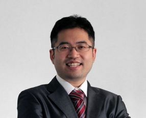
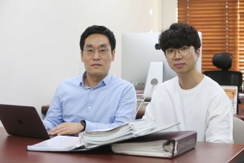
< Professor Sang Kil Cha > < Masters Candidate Kangsu Kim and Researcher Corentin Soulet > Team Geumo, led by Professor Sang Kil Cha from the Graduate School of Information Security, won the K-Cyber Security Challenge in the AI-based automatic vulnerability detection division for two consecutive years in 2018 and 2019. The K-Cyber Security Challenge is an inter-machine hacking competition. Participants develop and operate AI-based systems that are capable of independently identifying software vulnerabilities and gaining operating rights through hacking. The K-Cyber Security Challenge, inspired by the US Cyber Grand Challenge launched by the Defense Advanced Research Projects Agency (DARPA), is hosted by the Ministry of Science and ICT and organized by the Korea Internet and Security Agency. Researcher Corentin Soulet of the School of Computing and master’s student Kangsu Kim of the Graduate School of Information Security teamed up for the competition. Professor Cha, who has led the research on software and systems security since his days at Carnegie Mellon University, succeeded in establishing a world-class system using domestic technology. In a recent collaboration with the Cyber Security Research Center, Professor Cha achieved a ten-fold increase in the speed of binary analysis engines, a key component of AI-based hacking systems. For this accomplishment, he received the Best Paper Award at the 2019 Network and Distributed System Security Workshop on Binary Analysis Research (NDSS BAR). Kangsu Kim said, "It is a great honor to win the competition two years in a row. I will continue to work hard and apply my knowledge to serve society.”
-
Two Professors Receive Awards from the Korea Robot..
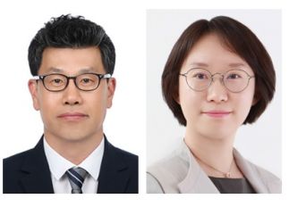
< Professor Jee-Hwan Ryu and Professor Ayoung Kim > The Korea Robotics Society (KROS), in recognition of their achievements and contributions to the development of robotic technology and industry in 2019, awarded two KAIST professors from the Department of Civil and Environmental Engineering. Professor Jee-Hwan Ryu has been actively engaged in researching the field of teleoperation, and this led him to win the KROS Robotics Innovation (KRI) Award. The KRI Award was newly established in 2019 by the KROS, in order to encourage researchers who have made innovative achievements in robotics. Professor Ryu shared the honor of being the first winners of this award with Professor Jaeheung Park of Seoul National University. Professor Ayoung Kim, from the same department, received the Young Investigator Award presented to emerging robitics researchers under 40 years of age.
-
New Liquid Metal Wearable Pressure Sensor Created ..
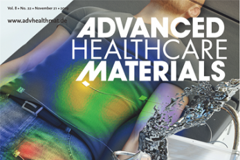
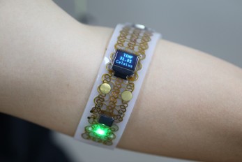
Soft pressure sensors have received significant research attention in a variety of fields, including soft robotics, electronic skin, and wearable electronics. Wearable soft pressure sensors have great potential for the real-time health monitoring and for the early diagnosis of diseases. A KAIST research team led by Professor Inkyu Park from the Department of Mechanical Engineering developed a highly sensitive wearable pressure sensor for health monitoring applications. This work was reported in Advanced Healthcare Materials on November 21 as a front cover article. This technology is capable of sensitive, precise, and continuous measurement of physiological and physical signals and shows great potential for health monitoring applications and the early diagnosis of diseases. A soft pressure sensor is required to have high compliance, high sensitivity, low cost, long-term performance stability, and environmental stability in order to be employed for continuous health monitoring. Conventional solid-state soft pressure sensors using functional materials including carbon nanotubes and graphene have showed great sensing performance. However, these sensors suffer from limited stretchability, signal drifting, and long-term instability due to the distance between the stretchable substrate and the functional materials. To overcome these issues, liquid-state electronics using liquid metal have been introduced for various wearable applications. Of these materials, Galinstan, a eutectic metal alloy of gallium, indium, and tin, has great mechanical and electrical properties that can be employed in wearable applications. But today’s liquid metal-based pressure sensors have low-pressure sensitivity, limiting their applicability for health monitoring devices. The research team developed a 3D-printed rigid microbump array-integrated, liquid metal-based soft pressure sensor. With the help of 3D printing, the integration of a rigid microbump array and the master mold for a liquid metal microchannel could be achieved simultaneously, reducing the complexity of the manufacturing process. Through the integration of the rigid microbump and the microchannel, the new pressure sensor has an extremely low detection limit and enhanced pressure sensitivity compared to previously reported liquid metal-based pressure sensors. The proposed sensor also has a negligible signal drift over 10,000 cycles of pressure, bending, and stretching and exhibited excellent stability when subjected to various environmental conditions. These performance outcomes make it an excellent sensor for various health monitoring devices. First, the research team demonstrated a wearable wristband device that can continuously monitor one’s pulse during exercise and be employed in a noninvasive cuffless BP monitoring system based on PTT calculations. Then, they introduced a wireless wearable heel pressure monitoring system that integrates three 3D-BLiPS with a wireless communication module. Professor Park said, “It was possible to measure health indicators including pulse and blood pressure continuously as well as pressure of body parts using our proposed soft pressure sensor. We expect it to be used in health care applications, such as the prevention and the monitoring of the pressure-driven diseases such as pressure ulcers in the near future. There will be more opportunities for future research including a whole-body pressure monitoring system related to other physical parameters.” This work was supported by a National Research Foundation of Korea (NRF) grant funded by the Ministry of Science and ICT. < Figure 1. The front cover image of Advanced Healthcare Materials, Volume 8, Issue 22. > < Figure 2. Highly sensitive liquid metal-based soft pressure sensor integrated with 3D-printed microbump array. > < Figure 3. High pressure sensitivity and reliable sensing performances of the proposed sensor and wireless heel pressure monitoring application. > Profile: Prof. Inkyu Park inkyu@kaist.ac.kr Micro/Nano Transducers Laboratory http://mintlab1.kaist.ac.kr/ Department of Mechanical Engineering KAIST
-
New IEEE Fellow, Professor Jong Chul Ye
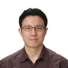
(Professor Jong Chul Ye at the Department of Bio and Brain Engineering) Professor Jong Chul Ye from the Department of Bio and Brain Engineering was named a new fellow of the Institute of Electrical and Electronics Engineers (IEEE). IEEE announced this on December 1 in recognition of Professor Ye’s contributions to the development of signal processing and artificial intelligence (AI) technology in the field of biomedical imaging. As the world’s largest society in the electrical and electronics field, IEEE names the top 0.1% of their members as fellows based on their research achievements.Professor Ye has published more than 100 research papers in world-leading journals in the biomedical imaging field, including those affiliated with IEEE. He also gave a keynote talk at the yearly conference of the International Society for Magnetic Resonance Imaging (ISMRM) on medical AI technology. In addition, Professor Ye has been appointed to serve as the next chair of the Computational Imaging Technical Committee of the IEEE Signal Processing Society, and the chair of the IEEE Symposium on Biomedical Imaging (ISBI) 2020 to be held in April in Iowa, USA. Professor Ye said, “The importance of AI technology is developing in the biomedical imaging field. I feel proud that my contributions have been internationally recognized and allowed me to be named an IEEE fellow.”
-
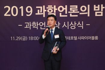
Professor Il-Doo Kim Named Scientist of the Year b..
(Professor Il-Doo Kim from the Department of Materials Science and Engineering) Professor Il-Doo Kim from the Department of Materials Science and Engineering was named the 2019 Scientist of the Year by Korean science journalists. The award was conferred at the 2019 Science Press Night ceremony of the Korea Science Journalists Association (KSJA) on November 29. Professor Kim focuses on developing nanofiber gas sensors for diagnosing diseases in advance by analyzing exhaled biomarkers with electrospinning technology. His outstanding research was praised and selected as one of the top 10 nanotechnology of 2019 by the Korea Nano Technology Research Society (KoNTRS), the Ministry of Science and ICT (MSIT), and the Ministry of Trade, Industry and Energy (MOTIE). Professor Kim was honored with the QIAN Baojun Fiber Award, which is awarded every two years by Donghua University in Shanghai, China to recognize outstanding contributions in fiber science and technology. Professor Kim was also elected as an academician of the Asia Pacific Academy of Materials (APAM) on November 21 in Guangzhou, China. In May, Professor Kim was appointed as an associate editor of ACS Nano, a leading international research journal in the field of nanoscience. In his editorial published in the May issue of ACS Nano, Professor Kim introduced and shared the history of KAIST and its vision for the future with other members of the journal. He hopes this will help with promoting a closer relationship between the members of the journal and KAIST moving forward. “Above all,” he said in his acceptance speech, “the greatest news for me as an educator is that the first PhD graduate from our lab, Dr. Seonjin Choi, was appointed as the youngest professor in the Division of Materials Science and Engineering at Hanyang University on September 1.”
-
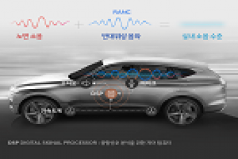
A System Controlling Road Active Noise to Hit the ..
The research team led by Professor Youngjin Park of the Department of Mechanical Engineering has developed a road noise active noise control (RANC) system to be commercialized in partnership with Hyundai Motor Group. On December 11, Hyundai Motor Group announced the successful development of the RANC system, which significantly reduces the road noise flowing into cars. The carmaker has completed the domestic and American patent applications for the location of sensors and the signal selection method, the core technology of RANC. RANC is a technology for reducing road noise during driving. This system consists of an acceleration sensor, digital signal processor (the control computer to analyze sound signals), microphone, amplifier, and audio system. To make the system as simple as possible, the audio system utilizes the original audio system embedded in the car instead of a separate system. The acceleration sensor first calculates the vibration from the road into the car. The location of the sensor is important for accurately identifying the vibration path. The research team was able to find the optimal sensor location through a number of tests. The System Dynamics and Applied Control Laboratory of Professor Park researched ways to significantly reduce road noise with Hyundai Motor Group for four years from 1993 as a G7 national project and published the results in international journals. In 2002, the researchers published an article titled “Noise Quietens Driving” in Nature, where they announced the first success in reducing road noise in actual cars. The achievement did not lead to commercialization, however, due to the lack of auxiliary technologies at the time, digital amplifiers and DSP for cars for example, and pricing issues. Since 2013, Professor Park’s research team has participated in one technology transfer and eight university-industry projects. Based on these efforts, the team was able to successfully develop the RANC system with domestic technology in partnership with Hyundai’s NVH Research Lab (Research Fellow, Dr. Gangdeok Lee; Ph.D. in aviation engineering, 1996), Optomech (Founder, Professor Gyeongsu Kim; Ph.D. in mechanical engineering, 1999), ARE (CEO Hyeonseok Kim; Ph.D. in mechanical engineering, 1998), WeAcom, and BurnYoung. Professor Park’s team led the project by performing theory-based research during the commercialization stage in collaboration with Hyundai Motor Group. For the commercialization of the RANC system, Hyundai Motor Group is planning to collaborate with the global car audio company Harman to increase the degree of completion and apply the RANC system to the GV 80, the first SUV model of the Genesis brand. “I am very delighted as an engineer to see the research I worked on from my early days at KAIST be commercialized after 20 years,” noted Professor Park. “I am thrilled to make a contribution to such commercialization with my students in my lab.”
-
New Members of KAST 2020
< Professor Zong-Tae Bae (Left) and Professor Sang Ouk Kim (Right) > Professor Zong-Tae Bae from the School of Management Engineering and Professor Sang Ouk Kim from the Department of Materials Science and Engineering became new fellows of the Korean Academy of Science and Technology (KAST) along with 22 other scientists in Korea. On November 22, KAST announced 24 new members for the year 2020. This includes seven scientists from the field of natural sciences, six from engineering, four from medical sciences, another four from policy research, and three from agriculture and fishery. The new fellows will begin their term from January next year, and their fellowships wll be conferred during the KAST’s New Year Reception to be held on January 14 in Seoul.
-
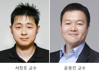
KAIST and Google Jointly Develop AI Curricula
KAIST selected the two professors who will develop AI curriculum under the auspices of the KAIST-Google Partnership for AI Education and Research. The Graduate School of AI announced the two authors among the 20 applicants who will develop the curriculum next year. They will be provided 7,500 USD per subject. Professor Changho Suh from the School of Electrical Engineering and Professor Yong-Jin Yoon from the Department of Mechanical Engineering will use Google technology such as TensorFlow, Google Cloud, and Android to create the curriculum. Professor Suh’s “TensorFlow for Information Theory and Convex Optimization “will be used for curriculum in the graduate courses and Professor Yoon’s “AI Convergence Project Based Learning (PBL)” will be used for online courses. Professor Yoon’s course will explore and define problems by utilizing AI and experiencing the process of developing products that use AI through design thinking, which involves product design, production, and verification. Professor Suh’s course will discus“information theory and convergence,” which uses basic sciences and engineering as well as AI, machine learning, and deep learning.
-
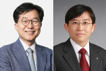
‘Carrier-Resolved Photo-Hall’ to Push Semiconducto..
(Professor Shin and Dr. Gunawan (left)) An IBM-KAIST research team described a breakthrough in a 140-year-old mystery in physics. The research reported in Nature last month unlocks the physical characteristics of semiconductors in much greater detail and aids in the development of new and improved semiconductor materials. Research team under Professor Byungha Shin at the Department of Material Sciences and Engineering and Dr. Oki Gunawan at IBM discovered a new formula and technique that enables the simultaneous extraction of both majority and minority carrier information such as their density and mobility, as well as gain additional insights about carrier lifetimes, diffusion lengths, and the recombination process. This new discovery and technology will help push semiconductor advances in both existing and emerging technologies. Semiconductors are the basic building blocks of today’s digital electronics age, providing us with a multitude of devices that benefit our modern life. To truly appreciate the physics of semiconductors, it is very important to understand the fundamental properties of the charge carriers inside the materials, whether those particles are positive or negative, their speed under an applied electric field, and how densely they are packed into the material. Physicist Edwin Hall found a way to determine those properties in 1879, when he discovered that a magnetic field will deflect the movement of electronic charges inside a conductor and that the amount of deflection can be measured as a voltage perpendicular to the flow of the charge. Decades after Hall’s discovery, researchers also recognized that they can measure the Hall effect with light via “photo-Hall experiments”. During such experiments, the light generates multiple carriers or electron–hole pairs in the semiconductors. Unfortunately, the basic Hall effect only provided insights into the dominant charge carrier (or majority carrier). Researchers were unable to extract the properties of both carriers (the majority and minority carriers) simultaneously. The property information of both carriers is crucial for many applications that involve light such as solar cells and other optoelectronic devices. In the photo-Hall experiment by the KAIST-IBM team, both carriers contribute to changes in conductivity and the Hall coefficient. The key insight comes from measuring the conductivity and Hall coefficient as a function of light intensity. Hidden in the trajectory of the conductivity, the Hall coefficient curve reveals crucial new information: the difference in the mobility of both carriers. As discussed in the paper, this relationship can be expressed elegantly as: Δµ = d (σ²H)/dσ The research team solved for both majority and minority carrier mobility and density as a function of light intensity, naming the new technique Carrier-Resolved Photo Hall (CRPH) measurement. With known light illumination intensity, the carrier lifetime can be established in a similar way. Beyond advances in theoretical understanding, advances in experimental techniques were also critical for enabling this breakthrough. The technique requires a clean Hall signal measurement, which can be challenging for materials where the Hall signal is weak due to low mobility or when extra unwanted signals are present, such as under strong light illumination. The newly developed photo-Hall technique allows the extraction of an astonishing amount of information from semiconductors. In contrast to only three parameters obtained in the classic Hall measurements, this new technique yields up to seven parameters at every tested level of light intensity. These include the mobility of both the electron and hole; their carrier density under light; the recombination lifetime; and the diffusion lengths for electrons, holes, and ambipolar types. All of these can be repeated N times (i.e. the number of light intensity settings used in the experiment). Professor Shin said, “This novel technology sheds new light on understanding the physical characteristics of semiconductor materials in great detail.” Dr. Gunawan added, “This will will help accelerate the development of next-generation semiconductor technology such as better solar cells, better optoelectronics devices, and new materials and devices for artificial intelligence technology.” Profile: Professor Byungha Shin Department of Materials Science and Engineering KAIST byungha@kaist.ac.kr http://energymatlab.kaist.ac.kr/
-
AI to Determine When to Intervene with Your Drivin..
(Professor Lee Uichin(left) and PhD candidate Auk Kim) Can your AI agent judge when to talk to you while you are driving? According to a KAIST research team, their in-vehicle conservation service technology will judge when it is appropriate to contact you to ensure your safety. Professor Uichin Lee from the Department of Industrial and Systems Engineering at KAIST and his research team have developed AI technology that automatically detects safe moments for AI agents to provide conversation services to drivers. Their research focuses on solving the potential problems of distraction created by in-vehicle conversation services. If an AI agent talks to a driver at an inopportune moment, such as while making a turn, a car accident will be more likely to occur. In-vehicle conversation services need to be convenient as well as safe. However, the cognitive burden of multitasking negatively influences the quality of the service. Users tend to be more distracted during certain traffic conditions. To address this long-standing challenge of the in-vehicle conversation services, the team introduced a composite cognitive model that considers both safe driving and auditory-verbal service performance and used a machine-learning model for all collected data. The combination of these individual measures is able to determine the appropriate moments for conversation and most appropriate types of conversational services. For instance, in the case of delivering simple-context information, such as a weather forecast, driver safety alone would be the most appropriate consideration. Meanwhile, when delivering information that requires a driver response, such as a “Yes” or “No,” the combination of driver safety and auditory-verbal performance should be considered. The research team developed a prototype of an in-vehicle conversation service based on a navigation app that can be used in real driving environments. The app was also connected to the vehicle to collect in-vehicle OBD-II/CAN data, such as the steering wheel angle and brake pedal position, and mobility and environmental data such as the distance between successive cars and traffic flow. Using pseudo-conversation services, the research team collected a real-world driving dataset consisting of 1,388 interactions and sensor data from 29 drivers who interacted with AI conversational agents. Machine learning analysis based on the dataset demonstrated that the opportune moments for driver interruption could be correctly inferred with 87% accuracy. The safety enhancement technology developed by the team is expected to minimize driver distractions caused by in-vehicle conversation services. This technology can be directly applied to current in-vehicle systems that provide conversation services. It can also be extended and applied to the real-time detection of driver distraction problems caused by the use of a smartphone while driving. Professor Lee said, “In the near future, cars will proactively deliver various in-vehicle conversation services. This technology will certainly help vehicles interact with their drivers safely as it can fairly accurately determine when to provide conversation services using only basic sensor data generated by cars.” The researchers presented their findings at the ACM International Joint Conference on Pervasive and Ubiquitous Computing (Ubicomp’19) in London, UK. This research was supported in part by Hyundai NGV and by the Next-Generation Information Computing Development Program through the National Research Foundation of Korea (NRF) funded by the Ministry of Science and ICT. (Figure: Visual description of safe enhancement technology for in-vehicle conversation services)
-
Transformative Electronics Systems to Broaden Wear..
Imagine a handheld electronic gadget that can soften and deform when attached to our skin. This will be the future of electronics we all dreamed of. A research team at KAIST says their new platform called 'Transformative Electronics Systems' will open a new class of electronics, allowing reconfigurable electronic interfaces to be optimized for a variety of applications. A team working under Professor Jae-Woong Jeong from the School of Electrical Engineering at KAIST has invented a multifunctional electronic platform that can mechanically transform its shape, flexibility, and stretchability. This platform, which was reported in Science Advances, allows users to seamlessly and precisely tune its stiffness and shape. "This new class of electronics will not only offer robust, convenient interfaces for use in both tabletop or handheld setups, but also allow seamless integration with the skin when applied onto our bodies," said Professor Jeong. The transformative electronics consist of a special gallium metal structure, hermetically encapsulated and sealed within a soft silicone material, combined with electronics that are designed to be flexible and stretchable. The mechanical transformation of the electronic systems is specifically triggered by temperature change events controlled by the user. "Gallium is an interesting key material. It is biocompatible, has high rigidity in solid form, and melts at a temperature comparable to the skin's temperature," said lead author Sang-Hyuk Byun, a researcher at KAIST. Once the transformative electronic platform comes in contact with a human body, the gallium metal encapsulated inside the silicone changes to a liquid state and softens the whole electronic structure, making it stretchable, flexible, and wearable. The gallium metal then solidifies again once the structure is peeled off the skin, making the electronic circuits stiff and stable. When flexible electronic circuits were integrated onto these transformative platforms, it empowered them with the ability to become either flexible and stretchable or rigid. "This technology could not have been achieved without interdisciplinary efforts," said co-lead author Joo Yong Sim, who is a researcher with ETRI. "We worked together with electrical, mechanical, and biomedical engineers, as well as material scientists and neuroscientists to make this breakthrough." This universal electronics platform allowed researchers to demonstrate applications that were highly adaptable and customizable, such as a multi-purpose personal electronics with variable stiffness and stretchability, a pressure sensor with tuneable bandwidth and sensitivity, and a neural probe that softens upon implantation into brain tissue. Applicable for both traditional and emerging electronics technologies, this breakthrough can potentially reshape the consumer electronics industry, especially in the biomedical and robotic domains. The researchers believe that with further development, this novel electronics technology can significantly impact the way we use electronics in our daily life. < Transformative electronics in soft mode, which becomes wearable for outdoor applications.> Video Material: https://youtu.be/im0J18TfShk Publication: Sang-Hyuk Byun, Joo Yong Sim, Zhanan Zhou, Juhyun Lee, Raza Qazi, Marie C. Walicki, Kyle E. Parker, Matthew P. Haney, Su Hwan Choi, Ahnsei Shon, Graydon B. Gereau, John Bilbily, Shuo Li, Yuhao Liu, Woon-Hong Yeo, Jordan G. McCall, Jianliang Xiao, and Jae-Woong Jeong. 2019. Mechanically transformative electronics, sensors, and implantable devices. Science Advances. Volume 5. No. 11. 12 pages. https://doi.org/10.1126/sciadv.aay0418 Link to download the full-text paper: https://advances.sciencemag.org/content/advances/5/11/eaay0418.full.pdf Profile: Prof. Jae-Woong Jeong, PhD jjeong1@kaist.ac.kr https://www.jeongresearch.org/ Professor Bio-Integrated Electronics and Systems Laboratory School of Electrical Engineering Korea Advanced Institute of Science and Technology (KAIST) https://www.kaist.ac.kr Daejeon 34141, Korea Profile: Sang-Hyuk Byun, PhD Candidate shbun95@kaist.ac.kr
-
Professor Byong-Guk Park Named Scientist of Octobe..
< Professor Byong-Guk Park > Professor Byong-Guk Park from the Department of Materials Science and Engineering was selected as the ‘Scientist of the Month’ for October 2019 by the Ministry of Science and ICT and the National Research Foundation of Korea. Professor Park was recognized for his contributions to the advancement of spin-orbit torque (SOT)-based magnetic random access memory (MRAM) technology. He received 10 million KRW in prize money. A next-generation, non-volatile memory device MRAM consists of thin magnetic films. It can be applied in “logic-in-memory” devices, in which logic and memory functionalities coexist, thus drastically improving the performance of complementary metal-oxide semiconductor (CMOS) processors. Conventional MRAM technology is limited in its ability to increase the operation speed of a memory device while maintaining a high density. Professor Park tackled this challenge by introducing a new material, antiferromagnet (IrMn), that generates a sizable amount of SOT as well as an exchange-bias field, which makes successful data writing possible without an external magnetic field. This research outcome paved the way for the development of MRAM, which has a simple device structure but features high speeds and density. Professor Park said, “I feel rewarded to have forwarded the feasibility and applicability of MRAM. I will continue devoting myself to studying further on the development of new materials that can help enhance the performance of memory devices."
![]()
291 Daehak-ro, Yuseong-gu, Daejeon, Korea 34141
KAIST College of Engineering
T.+82-42-350-2114
F.+82-42-350-2210 (2220)
ⓒ KAIST College of Engineering. All rights reserved.