Kaist
Korean

Faculty News
-
KAIST Unveils the Hidden Control Architecture of B..
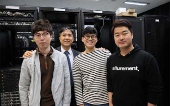
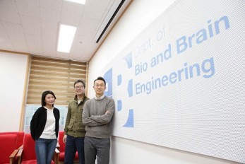
(Professor Kwang-Hyun Cho and his team) A KAIST research team identified the intrinsic control architecture of brain networks. The control properties will contribute to providing a fundamental basis for the exogenous control of brain networks and, therefore, has broad implications in cognitive and clinical neuroscience. Although efficiency and robustness are often regarded as having a trade-off relationship, the human brain usually exhibits both attributes when it performs complex cognitive functions. Such optimality must be rooted in a specific coordinated control of interconnected brain regions, but the understanding of the intrinsic control architecture of brain networks is lacking. Professor Kwang-Hyun Cho from the Department of Bio and Brain Engineering and his team investigated the intrinsic control architecture of brain networks. They employed an interdisciplinary approach that spans connectomics, neuroscience, control engineering, network science, and systems biology to examine the structural brain networks of various species and compared them with the control architecture of other biological networks, as well as man-made ones, such as social, infrastructural and technological networks. In particular, the team reconstructed the structural brain networks of 100 healthy human adults by performing brain parcellation and tractography with structural and diffusion imaging data obtained from the Human Connectome Project database of the US National Institutes of Health. The team developed a framework for analyzing the control architecture of brain networks based on the minimum dominating set (MDSet), which refers to a minimal subset of nodes (MD-nodes) that control the remaining nodes with a one-step direct interaction. MD-nodes play a crucial role in various complex networks including biomolecular networks, but they have not been investigated in brain networks. By exploring and comparing the structural principles underlying the composition of MDSets of various complex networks, the team delineated their distinct control architectures. Interestingly, the team found that the proportion of MDSets in brain networks is remarkably small compared to those of other complex networks. This finding implies that brain networks may have been optimized for minimizing the cost required for controlling networks. Furthermore, the team found that the MDSets of brain networks are not solely determined by the degree of nodes, but rather strategically placed to form a particular control architecture. Consequently, the team revealed the hidden control architecture of brain networks, namely, the distributed and overlapping control architecture that is distinct from other complex networks. The team found that such a particular control architecture brings about robustness against targeted attacks (i.e., preferential attacks on high-degree nodes) which might be a fundamental basis of robust brain functions against preferential damage of high-degree nodes (i.e., brain regions). Moreover, the team found that the particular control architecture of brain networks also enables high efficiency in switching from one network state, defined by a set of node activities, to another – a capability that is crucial for traversing diverse cognitive states. Professor Cho said, “This study is the first attempt to make a quantitative comparison between brain networks and other real-world complex networks. Understanding of intrinsic control architecture underlying brain networks may enable the development of optimal interventions for therapeutic purposes or cognitive enhancement.” This research, led by Byeongwook Lee, Uiryong Kang and Hongjun Chang, was published in iScience (10.1016/j.isci.2019.02.017) on March 29, 2019. Figure 1. Schematic of identification of control architecture of brain networks. Figure 2. Identified control architectures of brain networks and other real-world complex networks.
-

On-chip Drug Screening for Identifying Antibiotic ..
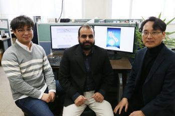
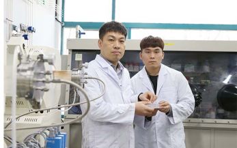
(from left: Seunggyu Kimand Professor Jessie Sungyun Jeon) A KAIST research team developed a microfluidic-based drug screening chip that identifies synergistic interactions between two antibiotics in eight hours. This chip can be a cell-based drug screening platform for exploring critical pharmacological patterns of antibiotic interactions, along with potential applications in screening other cell-type agents and guidance for clinical therapies. Antibiotic susceptibility testing, which determines types and doses of antibiotics that can effectively inhibit bacterial growth, has become more critical in recent years with the emergence of antibiotic-resistant pathogenic bacteria strains. To overcome the antibiotic-resistant bacteria, combinatory therapy using two or more kinds of antibiotics has been gaining considerable attention. However, the major problem is that this therapy is not always effective; occasionally, unfavorable antibiotic pairs may worsen results, leading to suppressed antimicrobial effects. Therefore, combinatory testing is a crucial preliminary process to find suitable antibiotic pairs and their concentration range against unknown pathogens, but the conventional testing methods are inconvenient for concentration dilution and sample preparation, and they take more than 24 hours to produce the results. To reduce time and enhance the efficiency of combinatory testing, Professor Jessie Sungyun Jeon from the Department of Mechanical Engineering, in collaboration with Professor Hyun Jung Chung from the Department of Biological Sciences, developed a high-throughput drug screening chip that generates 121 pairwise concentrations between two antibiotics. The team utilized a microfluidic chip with a sample volume of a few tens of microliters. This chip enabled 121 pairwise concentrations of two antibiotics to be automatically formed in only 35 minutes. They loaded a mixture of bacterial samples and agarose into the microchannel and injected reagents with or without antibiotics into the surrounding microchannel. The diffusion of antibiotic molecules from the channel with antibiotics to the one without antibiotics resulted in the formation of two orthogonal concentration gradients of the two antibiotics on the bacteria-trapping agarose gel. The team observed the inhibition of bacterial growth by the antibiotic orthogonal gradients over six hours with a microscope, and confirmed different patterns of antibiotic pairs, classifying the interaction types into either synergy or antagonism. Professor Jeon said, “The feasibility of microfluidic-based drug screening chips is promising, and we expect our microfluidic chip to be commercialized and utilized in near future.” This study, led by Seunggyu Kim, was published in Lab on a Chip (10.1039/c8lc01406j) on March 21, 2019. Figure 1. Back cover image for the “Lab on a Chip”. Figure 2. Examples of testing results using the microfluidic chips developed in this research.
-
Professor Seoktae KANG received an IDEA award from..
Seoktae KANG, an associate professor at the department of civil and environmental engineering, received JSWE-IDEA prize in March 8th at the spring conference of JSWE (Japan society of water environment). This award is supported by IDEA consulting group in Japan, and the award is given to middle-career Asian researchers on water engineering during the annual conference of JSWE. At the 2019 award ceremony, Prof. Kang presented his research work entitled “Ultra-fast electrochemical oxidation of micropollutants by flow-through conductive membrane system”, which proposed novel application of carbon nanotube-based hollow membrane-type electrodes to overcome the oxidation of electrodes, side-reaction of intermediates, and mass-transfer limitation of the existing system.
-
True-meaning Wearable Displays: Self-powered, Wash..
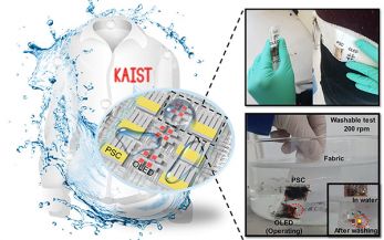
(Video: The washing process of wearing display module) When we think about clothes, they are usually formed with textiles and have to be both wearable and washable for daily use; however, smart clothing has had a problem with its power sources and moisture permeability, which causes the devices to malfunction. This problem has now been overcome by a KAIST research team, who developed a textile-based wearable display module technology that is washable and does not require an external power source. To ease out the problem of external power sources and enhance the practicability of wearable displays, Professor Kyung Cheol Choi from the School of Electrical Engineering and his team fabricated their wearing display modules on real textiles that integrated polymer solar cells (PSCs) with organic light emitting diodes (OLEDs). PSCs have been one of the most promising candidates for a next-generation power source, especially for wearable and optoelectronic applications because they can provide stable power without an external power source, while OLEDs can be driven with milliwatts. However, the problem was that they are both very vulnerable to external moisture and oxygen. The encapsulation barrier is essential for their reliability. The conventional encapsulation barrier is sufficient for normal environments; however, it loses its characteristics in aqueous environments, such as water. It limits the commercialization of wearing displays that must operate even on rainy days or after washing. To tackle this issue, the team employed a washable encapsulation barrier that can protect the device without losing its characteristics after washing through atomic layer deposition (ALD) and spin coating. With this encapsulation technology, the team confirmed that textile-based wearing display modules including PSCs, OLEDs, and the proposed encapsulation barrier exhibited little change in characteristics even after 20 washings with 10-minute cycles. Moreover, the encapsulated device operated stably with a low curvature radius of 3mm and boasted high reliability. Finally, it exhibited no deterioration in properties over 30 days even after being subjected to both bending stress and washing. Since it uses a less stressful textile, compared to conventional wearable electronic devices that use traditional plastic substrates, this technology can accelerate the commercialization of wearing electronic devices. Importantly, this wearable electronic device in daily life can save energy through a self-powered system. Professor Choi said, “I could say that this research realized a truly washable wearable electronic module in the sense that it uses daily wearable textiles instead of the plastic used in conventional wearable electronic devices. Saving energy with PSCs, it can be self-powered, using nature-friendly solar energy, and washed. I believe that it has paved the way for a ‘true-meaning wearable display’ that can be formed on textile, beyond the attachable form of wearable technology.” This research, in collaboration with Professor Seok Ho Cho from Chonnam National University and led by Eun Gyo Jeong, was published in Energy and Environmental Science (10.1039/c8ee03271h) on January 18, 2019. Figure 1. Schematic and photo of a washable wearing display module Figure 2. Cover page of Energy and Environmental Science
-
Distinguished Professor Sang Yup Lee Honored with ..
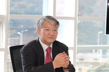
(Distinguished Professor Sang Yup Lee from the Department of Chemical and Biomolecular Engineering) Distinguished Professor Sang Yup Lee from the Department of Chemical and Biomolecular Engineering was honored to be the laureate of the 23rd NAEK Award. The NAEK (National Academy of Engineering of Korea) Award was instituted in 1997 to honor and recognize engineers who have made significant contributions to the development of the engineering and technology field at universities, industries, and institutions. Every year, it is conferred to only one person who has achieved original and world-leading research that has led to national development. Distinguished Professor Lee is a pioneering scholar of the field of systems metabolic engineering and he was recognized for his significant achievements in the biochemical industry by developing novel microbial bioprocesses. In particular, he is globally renowned for biological plastic synthesis, making or decomposing polymers with microorganisms instead of using fossil resources. He has produced numerous high-quality research breakthroughs in metabolic and systems engineering. In 2016, he produced an easily degradable plastic with Escherichia coli (E. coli). In 2018, he successfully produced aromatic polyesters, the main material for PET (poly ethylene terephthalate) from E. coli strains. He also identified microorganism structures for PET degradation and improved its degradability with a novel variant. His research was ranked number one in the research and development division of Top Ten Science and Technology News 2018 announced by Korean Federation of Science & Technology Societies. He is one of highly cited researchers (HCR) ranked in the top 1% by citations for their field by the Clarivate Analytics.
-

Wafer-scale multilayer fabrication of silk fibroin..
A KAIST research team developed a novel fabrication method for the multilayer processing of silk-based microelectronics. This technology for creating a biodegradable silk fibroin film allows microfabrication with polymer or metal structures manufactured from photolithography. It can be a key technology in the implementation of silk fibroin-based biodegradable electronic devices or localized drug delivery through silk fibroin patterns. Silk fibroins are biocompatible, biodegradable, transparent, and flexible, which makes them excellent candidates for implantable biomedical devices, and they have also been used as biodegradable films and functional microstructures in biomedical applications. However, conventional microfabrication processes require strong etching solutions and solvents to modify the structure of silk fibroins. To prevent the silk fibroin from being damaged during the process, Professor Hyunjoo J. Lee from the School of Electrical Engineering and her team came up with a novel process, named aluminum hard mask on silk fibroin (AMoS), which is capable of micropatterning multiple layers composed of both fibroin and inorganic materials, such as metal and dielectrics with high-precision microscale alignment. The AMoS process can make silk fibroin patterns on devices, or make patterns on silk fibroin thin films with other materials by using photolithography, which is a core technology in the current microfabrication process. The team successfully cultured primary neurons on the processed silk fibroin micro-patterns, and confirmed that silk fibroin has excellent biocompatibility before and after the fabrication process and that it also can be applied to implanted biological devices. Through this technology, the team realized the multilayer micropatterning of fibroin films on a silk fibroin substrate and fabricated a biodegradable microelectric circuit consisting of resistors and silk fibroin dielectric capacitors in a silicon wafer with large areas. They also used this technology to position the micro-pattern of the silk fibroin thin film closer to the flexible polymer-based brain electrode, and confirmed the dye molecules mounted on the silk fibroin were transferred successfully from the micropatterns. Professor Lee said, “This technology facilitates wafer-scale, large-area processing of sensitive materials. We expect it to be applied to a wide range of biomedical devices in the future. Using the silk fibroin with micro-patterned brain electrodes can open up many new possibilities in research on brain circuits by mounting drugs that restrict or promote brain cell activities.” This research, in collaboration with Dr. Nakwon Choi from KIST and led by PhD candidate Geon Kook, was published in ACS AMI (10.1021/acsami.8b13170) on January 16, 2019. Figure 1. The cover page of ACS AMI Figure 2. Fibroin microstructures and metal patterns on a fibroin produced by using the AMoS mask. Figure 3. Biocompatibility assessment of the AMoS Process. Top: Schematics image of a) fibroin-coated silicon b) fibroin-pattered silicon and c) gold-patterned fibroin. Bottom: Representative confocal microscopy images of live (green) and dead (red) primary cortical neurons cultured on the substrates.
-
Novel Material Properties of Hybrid Perovskite Nan..
(from left: Juho Lee, Dr. Muhammad Ejaz Khan and Professor Yong-Hoon Kim) A KAIST research team reported a novel non-linear device with the founding property coming from perovskite nanowires. They showed that hybrid perovskite-derived, inorganic-framework nanowires can acquire semi-metallicity, and proposed negative differential resistance (NDR) devices with excellent NDR characteristics that resulted from a novel quantum-hybridization NDR mechanism, implying the potential of perovskite nanowires to be realized in next-generation electronic devices. Organic-inorganic hybrid halide perovskites have recently emerged as prominent candidates for photonic applications due to their excellent optoelectronic properties as well as their low cost and facile synthesis processes. Prominent progresses have been already made for devices including solar cells, light-emitting diodes, lasers and photodetectors. However, research on electronic devices based on hybrid halide perovskites has not been actively pursued compared with their photonic device counterparts. Professor Yong-Hoon Kim from the School of Electrical Engineering and his team took a closer look at low-dimensional organic-inorganic halide perovskite materials, which have enhanced quantum confinement effects, and particularly focused on the recently synthesized trimethylsulfonium (TMS) lead triiodide (CH3)3SPbI3. Using supercomputer simulations, the team first showed that stripping the (CH3)3S or TMS organic ligands from the TMS PbI3 perovskite nanowires results in semi-metallic PbI3 columns, which contradicts the conventional assumption of the semiconducting or insulating characteristics of the inorganic perovskite framework. Utilizing the semi-metallic PbI3 inorganic framework as the electrode, the team designed a tunneling junction device from perovskite nanowires and found that they exhibit excellent nonlinear negative differential resistance (NDR) behavior. The NDR property is a key to realizing next-generation, ultra-low-power, and multivalued non-linear devices. Furthermore, the team found that this NDR originates from a novel mechanism that involves the quantum-mechanical hybridization between channel and electrode states. Professor Kim said, “This research demonstrates the potential of quantum mechanics-based computer simulations to lead developments in advanced nanomaterials and nanodevices. In particular, this research proposes a new direction in the development of a quantum mechanical tunneling device, which was the topic for which the Nobel Laureate in Physics in 1973 was awarded to Dr. Leo Esaki. This research, led by Dr. Muhammad Ejaz Khan and PhD candidate Juho Lee, was published online in Advanced Functional Materials (10.1002/adfm.201807620) on January 7, 2019. Figure. The draft version of the cover page of 'Advanced Functional Materials'
-
KAIST Develops Analog Memristive Synapses for Neur..
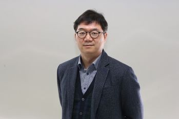
(Professor Sung-Yool Choi from the School of Electrical Engineering) A KAIST research team developed a technology that makes a transition of the operation mode of flexible memristors to synaptic analog switching by reducing the size of the formed filament. Through this technology, memristors can extend their role to memristive synapses for neuromorphic chips, which will lead to developing soft neuromorphic intelligent systems. Brain-inspired neuromorphic chips have been gaining a great deal of attention for reducing the power consumption and integrating data processing, compared to conventional semiconductor chips. Similarly, memristors are known to be the most suitable candidate for making a crossbar array which is the most efficient architecture for realizing hardware-based artificial neural network (ANN) inside a neuromorphic chip. A hardware-based ANN consists of a neuron circuit and synapse elements, the connecting pieces. In the neuromorphic system, the synaptic weight, which represents the connection strength between neurons, should be stored and updated as the type of analog data at each synapse. However, most memristors have digital characteristics suitable for nonvolatile memory. These characteristics put a limitation on the analog operation of the memristors, which makes it difficult to apply them to synaptic devices. Professor Sung-Yool Choi from the School of Electrical Engineering and his team fabricated a flexible polymer memristor on a plastic substrate, and found that changing the size of the conductive metal filaments formed inside the device on the scale of metal atoms can make a transition of the memristor behavior from digital to analog. Using this phenomenon, the team developed flexible memristor-based electronic synapses, which can continuously and linearly update synaptic weight, and operate under mechanical deformations such as bending. The team confirmed that the ANN based on these memristor synapses can effectively classify person’s facial images even when they were damaged. This research demonstrated the possibility of a neuromorphic chip that can efficiently recognize faces, numbers, and objects. Professor Choi said, “We found the principles underlying the transition from digital to analog operation of the memristors. I believe that this research paves the way for applying various memristors to either digital memory or electronic synapses, and will accelerate the development of a high-performing neuromorphic chip.” In a joint research project with Professor Sung Gap Im (KAIST) and Professor V. P. Dravid (Northwestern University), this study was led by Dr. Byung Chul Jang (Samsung Electronics), Dr. Sungkyu Kim (Northwestern University) and Dr. Sang Yoon Yang (KAIST), and was published online in Nano Letters on January 4, 2019. Figure 1. a) Schematic illustration of a flexible pV3D3 memristor-based electronic synapse array. b) Cross-sectional TEM image of the flexible pV3D3 memristor
-
New LSB with Theoretical Capacity over 90%
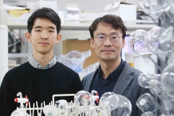
(Professor Hee-Tak Kim and Hyunwon Chu) A KAIST research team has developed a lithium sulfur battery (LSB) that realizes 92% of the theoretical capacity and an areal capacity of 4mAh/cm2. LSBs are gaining a great deal of attention as an alternative for lithium ion batteries (LIBs) because they have a theoretical energy density up to six to seven times higher than that of LIBs, and can be manufactured in a more cost-effective way. However, LSBs face the obstacle of having a capacity reaching its theoretical maximum because they are prone to uncontrolled growth of lithium sulfide on the electrodes, which leads to blocking electron transfer. To address the problem of electrode passivation, researchers introduced additional conductive agent into the electrode; however, it drastically lowered the energy density of LSBs, making it difficult to exceed 70% of the theoretical capacity. Professor Hee-Tak Kim from the Department of Chemical and Biomolecular Engineering and his team replaced the lithium salt anions used in conventional LSB electrolytes with anions with a high donor number. The team successfully induced the three-dimensional growth of lithium sulfide on electrode surfaces and efficiently delayed the electrode passivation. Based on this electrolyte design, the research team achieved 92% of the theoretical capacity with their high-capacity sulfur electrode (4mAh/cm2), which is equivalent to that of conventional LIB cathode. Furthermore, they were able to form a stable passivation film on the surface of the lithium anode and exhibited stable operation over 100 cycles. This technology, which can be flexibly used with various types of sulfur electrodes, can mark a new milestone in the battery industry. Professor Kim said, “We proposed a new physiochemical principle to overcome the limitations of conventional LSBs. I believe our achievement of obtaining 90% of the LBSs’ theoretical capacity without any capacity loss after 100 cycles will become a new milestone.” This research, first-authored by Hyunwon Chu and Hyungjun Noh, was published in Nature Communications on January 14, 2019. It was also selected in the editor’s highlight for its outstanding achievements. Figure 1. Lithium sulfur growth and its deposition mechanism for different sulfide growth behaviors Figure 2. Capacity and cycle life characteristics of the LSBs
-
President Shin Speaks on Closing the Skills Gap at..
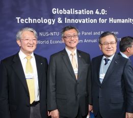
(President Shin poses (far right) with the National University of Singapore President Tan Eng Chye (center) along with Distinguished Professor Sang Yup Lee in Davos last week.) President Sung-Chul Shin shared his ideas on how reskilling is a critical element of growth, dynamism, and competitiveness for countries during a session titled “Closing the Skills Gap: Creating a Reskilling Revolution” at the World Economic Forum on January 24 in Davos. While discussing a reskilling imperative alongside French Labor Minister Muriel Penicaud, he presented how the Korean government and KAIST are responding to the socio-economic transformation of workforces in the Fourth Industrial Revolution. After their presentation, Minister of Economy and Enterprise of Spain Nadia Calvirno Santamaria, Minister of Commerce and Industry of Oman Ali bin Masoud bin Ali Al Sunaidy, and Minister of Petroleum and Natural Gas, Skill Development, and Entrepreneurship of India Dharmendra Pradhan shared their views on the course of decision making regarding the proactive practices and policies they have applied for closing the gaps from their countries’ perspectives. President Shin presented how to upskill and reskill SMEs and startups, the real players who will jumpstart the economy in the Fourth Industrial Revolution. He explained that the government is striving to change the existing structure of the economy, which is dominated by a few giant conglomerates. He added that the Korean government is trying to support SMEs and startups in terms of both funding and technology reskilling in order to rejuvenate the economy. To better align itself with the government’s efforts, KAIST has introduced SME 4.0. SME 4.0 proposes to innovate the production process through the creation of a partnered platform between KAIST and SMEs across the country. With this platform, KAIST assists local SMEs for standardizing and systemizing all their processes of production, delivery, and management with enterprise resources planning (ERP) and manufacturing execution systems (MES). In addition, SME 4.0 offers retraining and re-tooling programs by linking the data generated through this platform in real time to better facilitate SMEs’ smart business. (President Shin shakes hands with H.E.Mohammed Al-Tuwairi, Minister of Economy and Planning of Saudi Arabia before holding a bilaterla meeting in Davos.) President Shin also explained about upskilling the leading corporations’ technological competitiveness, partnering with major leading corporations for upskilling their advanced technologies. He also held a series of bilateral meetings with dignitaries attending the WEF annual meeting to discuss partnerships and collaborations. He also attended the Global University Leaders Forum (GULF), a community composed of 28 presidents from the world’s top universities on January 23. President Shin, who is on the advisory board of the Center for Fourth Industrial Revolution (C4IR), also participated in the board meeting and discussed the upcoming launching of the Korea C4IR, which will open at KAIST in March.
-
Hierarchical Porous Titanium Nitride Synthesized b..
(from left: Professor Jinwoo Lee and PhD candidate Won-Gwang Lim) A KAIST research team developed ultra-stable, high-rate lithium-sulfur batteries (LSBs) by using hierarchical porous titanium nitride as a sulfur host, and achieved superior cycle stability and high rate performance for LSBs. The control of large amounts of energy is required for use in an electric vehicle or smart grid system. In this sense, the development of next-generation secondary batteries is in high demand. Theoretically, LSBs have an energy density seven times higher than commercial lithium ion batteries (LIBs). Also, their production cost can be reduced dramatically since sulfur can be obtained at a low price. Despite these positive aspects, there have been several issues impeding the commercialization of LSBs, such as the low electric conductivity of sulfur, the dissolution of active materials during operation, and sluggish conversion reactions. These issues decrease the cycle stability and rate capability of batteries. To tackle those issues, Professor Jinwoo Lee from the Department of Chemical and Biomolecular Engineering and his team synthesized a well-developed hierarchical macro/mesoporous titanium nitride as a host material for sulfur. The titanium nitride has a high chemical affinity for sulfur and high electrical conductivity. As a result, it prevents the dissolution of active materials and facilitates the charge transfer. Moreover, the synergistic effect of macropore and mesopore structures allows the stable accommodation of large amounts of sulfur and facilitates the electrolyte penetration. Previously reported polar inorganic materials have a high affinity for sulfur, but it was challenging to control the porous architecture suitable to the sulfur host. This work breaks such limitations by developing a synthetic route to easily control the porous architecture of inorganic materials, which led to obtaining superior cycle stability and high rate capabilities. Professor Lee said, “Some problems still remain in commercializing LSBs as next-generation batteries. Hence, there should be a continued research on this matter to solve the issues. Through this research, we secured a key technology for ultrastable, high-rate LSBs.” This research was led by PhD candidate Won-Gwang Lim and collaborated on by Jeong Woo Han from POSTECH. It was chosen as the cover article of Advanced Materials on January 15, 2019. Figure 1. Schematic illustration for the synthetic route of co-continuous h-TiN Figure 2. The hierarchical multiscale porous structure is still retained without any collapse after the conversion to h-TiN. The good retention of the porous structure is attributed to the thick pore wall of the h-TiO₂derived from the block copolymer self-assembly Figure 3. The cover page of Advanced Materials
-
Brain-inspired Artificial Intelligence in Robots
Research groups in KAIST, the University of Cambridge, Japan’s National Institute for Information and Communications Technology, and Google DeepMind argue that our understanding of how humans make intelligent decisions has now reached a critical point in which robot intelligence can be significantly enhanced by mimicking strategies that the human brain uses when we make decisions in our everyday lives. Despite the rapid progress being made in strengthening the physical capability of robots, their central control systems, which govern how robots decide what to do at any one time, are still inferior to those of humans. In particular, they often rely on pre-programmed instructions to direct their behavior, and lack the hallmark of human behavior, that is, the flexibility and capacity to quickly learn and adapt. The problem with importing human-like intelligence into robots has always been a difficult task without knowing the computational principles for how the human brain makes decisions –in other words, how to translate brain activity into computer code for the robots’ ‘brains’. The team argued that this inter-disciplinary approach will provide just as many benefits to neuroscience as to robotics. The recent explosion of interest in what lies behind psychiatric disorders such as anxiety, depression, and addiction has given rise to a set of sophisticated theories that are complex and difficult to test without some sort of advanced situation platform. how it interacts with the world in real-life to test whether and how different abnormalities in these models give rise to certain disorders. For instance, if we could reproduce anxiety behavior or obsessive-compulsive disorder in a robot, we could then predict what we need to do to treat it in humans.” Professor Seymour said, “We might think that having robots with the human traits of being a bit impulsive or overcautious would be a detriment, but these traits are an unavoidable by-product of human-like intelligence. And it turns out that this is helping us to understand human behavior as human.” <span style="font-family:;" times="" new="" roman";="" 9pt;"="" 12pt;"="">The framework for achieving this brain-inspired artificial intelligence was published in two journals, Science Robotics (10.1126/scirobotics.aav2975) on January 16 and Current Opinion in Behavioral Sciences (10.1016/j.cobeha.2018.12.012) on February 6, 2019. Figure 1. Overview of neuroscience - robotics approach for decision-making. The figure details key areas for interdisciplinary study (Current Opinion in Behavioral Sciences) Figure 2. Brain-inspired solutions to robot learning. Neuroscientific views on various aspects of learning and cognition converge and create a new idea called prefrontal metacontrol, which can inspire researchers to design learning agents that can address various key challenges in robotics such as performance-efficiency-speed, cooperation-competition, and exploration-exploitation trade-offs (Science Robotics)

